Precision ion polishing system and sample clamp thereof

A sample and ion technology, applied in the field of semiconductor and precision ion milling machines, can solve the problems of sample breakage, affecting production efficiency, wasting manpower and material resources, and achieving the effect of avoiding excessive grinding, saving manpower and material resources, and improving production efficiency.

Inactive Publication Date: 2010-11-03
SEMICON MFG INT (SHANGHAI) CORP
View PDF0 Cites 7 Cited by
  • Summary
  • Abstract
  • Description
  • Claims
  • Application Information

AI Technical Summary

Problems solved by technology

Therefore, when the precision ion milling machine in the prior art further thins the TEM sample, it often encounters such a problem: the sample has been excessively ground and damaged, and the structure to be observed is still at the thicker edge of the damaged part.
However, since the...

Method used


Image

  • Precision ion polishing system and sample clamp thereof
  • Precision ion polishing system and sample clamp thereof
  • Precision ion polishing system and sample clamp thereof

Examples


Embodiment Construction

[0024] The present invention will be described in further detail below in conjunction with the accompanying drawings.

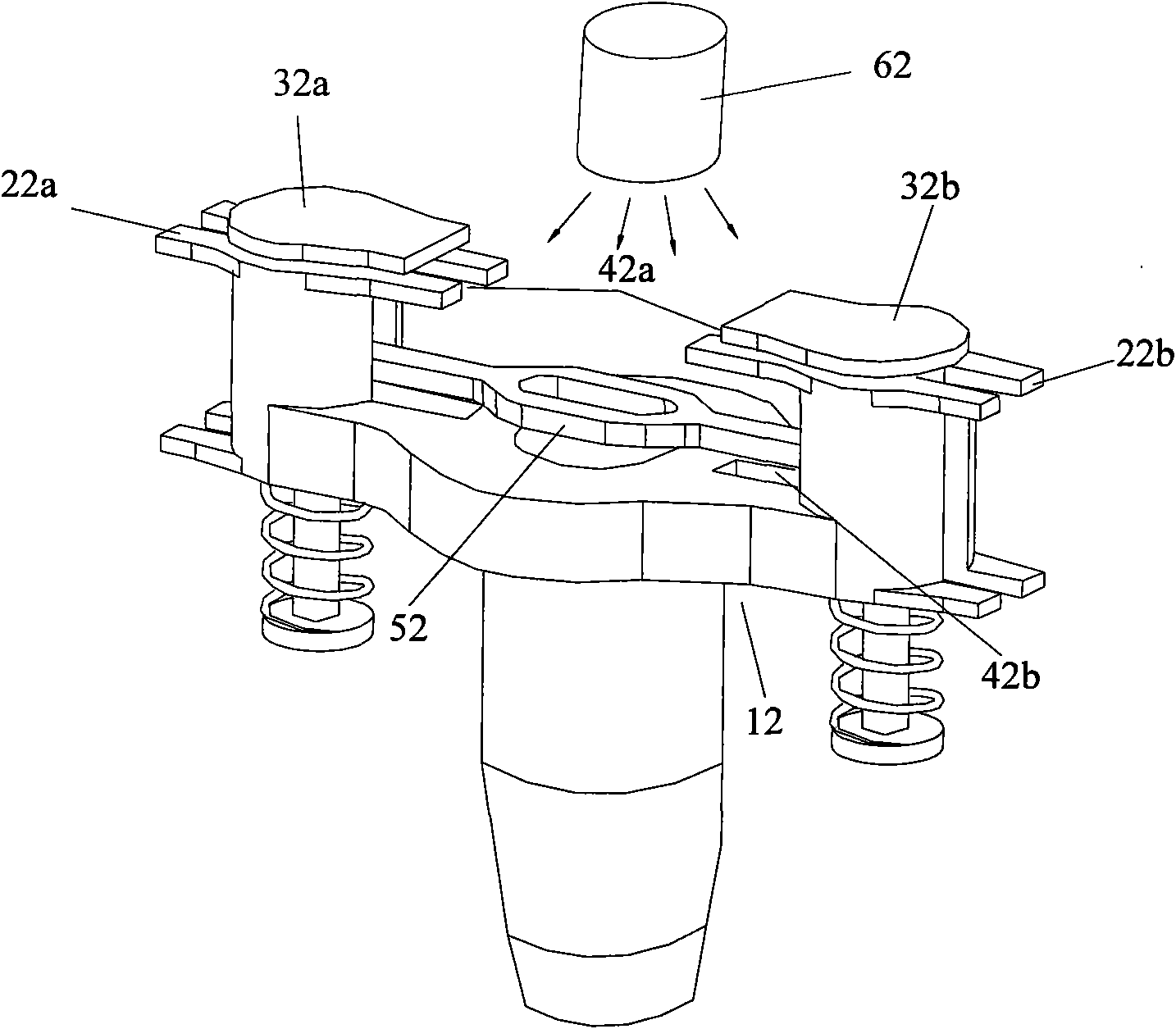
[0025] The first aspect of the present invention provides a sample holder for a precision ion mill table, which includes one or more clips, and the one or more clips can move in their respective horizontal planes to adjust the relative The fixed position of the ion beam on the precision ion machine. The sample holder also includes one or more control devices for controlling the movement of the clip in its own plane.

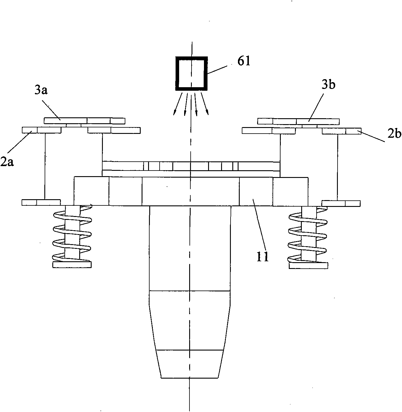
[0026] figure 2 A schematic structural view of a sample holder for a precision ion mill according to a specific embodiment of the present invention. For the convenience of description, this embodiment is only described in the case that the sample holder includes two clips, but those skilled in the art should understand that there is no strict limit on the number of clips in practical applications, as long as the clips included in the sample h...


PUM

PropertyMeasurementUnit
Lengthaaaaaaaaaa
Lengthaaaaaaaaaa
Lengthaaaaaaaaaa

Abstract

The invention provides a precision ion polishing system and a sample clamp thereof. The precision ion polishing system comprises one or more clamping pieces which can move in planes of the clamping pieces so as to adjust the fixed positions of samples relative to ion beams of the precision ion polishing system. The invention also provides the precision ion polishing system, which comprises the sample clamps provided by the embodiment. The precision ion polishing system and the sample clamp thereof can adjust the positions of the TEM samples relative to ion guns of the precision ion polishing system so as to effectively avoid the condition that the samples are excessively polished even damaged while structures to be observed are still on the relatively thicker parts of damaged edges.

Description

technical field [0001] The invention relates to the field of semiconductors, in particular to the field of precision ion milling machines. Background technique [0002] In the field of semiconductor manufacturing, TEM samples are an important tool for detecting the shape, size and characteristics of device films. The working principle of using TEM samples to detect device films is to thin the TEM samples to be tested to less than 0.2 microns , and then placed in the TEM observation room, the sample is irradiated with a high-voltage accelerated electron beam to enlarge the shape of the TEM sample, and then projected on the screen and photographed for analysis. One of the outstanding advantages of TEM samples is that they have high resolution and can observe the morphology and size of extremely thin films. Due to the extremely thin gate oxide layer of semiconductor devices below 0.35 micron process, TEM is currently the only equipment capable of precise measurement of this th...

Claims


Application Information

Patent Timeline
IPC IPC(8): G01N1/28G01N23/04
Inventor 虞勤琴高强胡建强王燕君
Owner SEMICON MFG INT (SHANGHAI) CORP
Why Eureka
Try Eureka