
Method for realizing selectivity through low temperature

A selective, low-temperature technology, applied in the fields of electrical components, semiconductor/solid-state device manufacturing, circuits, etc., can solve problems such as difficult exhaust gas treatment

Active Publication Date: 2010-11-10
TSINGHUA UNIV
View PDF2 Cites 0 Cited by
  • Summary
  • Abstract
  • Description
  • Claims
  • Application Information

AI Technical Summary

Problems solved by technology

[0006] The purpose of the present invention is to at least solve one of the above-mentioned technical defects, especially when epitaxy does not need to feed HCl gas, thereby avoiding problems such as difficulties in tail gas treatment caused by feeding HCl gas

Method used


Image

  • Method for realizing selectivity through low temperature
  • Method for realizing selectivity through low temperature
  • Method for realizing selectivity through low temperature

Examples


Embodiment Construction

[0014] The embodiments of the present invention are described in detail below. Examples of the embodiments are shown in the accompanying drawings, in which the same or similar reference numerals indicate the same or similar elements or elements with the same or similar functions. The embodiments described below with reference to the accompanying drawings are exemplary, and are only used to explain the present invention, and cannot be construed as limiting the present invention.

[0015] The following disclosure provides many different embodiments or examples for implementing different structures of the present invention. In order to simplify the disclosure of the present invention, the components and settings of specific examples are described below. Of course, they are only examples, and are not intended to limit the invention. In addition, the present invention may repeat reference numbers and / or letters in different examples. This repetition is for the purpose of simplificat...


PUM


Abstract

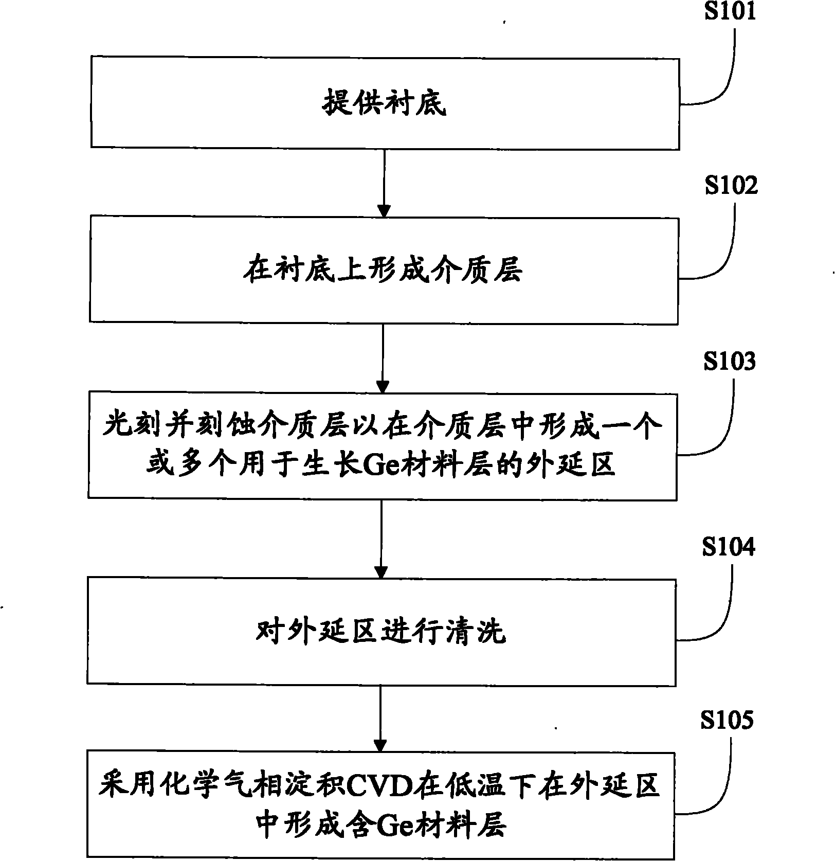
The invention provides a method for realizing selectivity through low temperature, which comprises the following steps: providing a substrate; forming a dielectric layer on the substrate; photoetching and etching the dielectric layer to form one or more epitaxial regions for growing Ge-containing material layers in the dielectric layer; and forming the Ge-containing material layers in the epitaxial regions under a low-temperature condition that chemical vapor deposition (CVD) is adopted and HCl is not introduced. In the embodiment of the invention, Ge-containing material layers are extended by a low temperature mode, thus at lower temperatures, the probability of nucleation of the epitaxial material on the dielectric layer is greatly reduced, and good selectivity can be realized without introducing the HCl gas, thereby avoiding the problems of pollution and the like caused by introduction of the HCl gas.

Description

Technical field [0001] The invention relates to the technical field of semiconductor manufacturing and design, in particular to a method for achieving selectivity through low temperature. Background technique [0002] In the semiconductor industry, silicon (Si) has been developed as a dominant semiconductor material for decades, during which time it has shown good performance. However, as the feature size of the device continues to shrink, the size of a single transistor has gradually reached the physical and technical limits. Therefore, the mobility of CMOS devices with silicon as the channel material has become lower and lower, which has been unable to meet the continuous performance of the device. Requirements for promotion. In order to solve this problem, the prior art introduces strain technology to improve the mobility of silicon materials, or directly uses other materials with higher mobility to replace Si as the channel material of the device, among which Ge materials ha...

Claims


Application Information

Patent Timeline
IPC IPC(8): H01L21/205
Inventor 王敬许军郭磊
Owner TSINGHUA UNIV
Learn More