Method for improving graphics critical dimension uniformity in mask

A key dimension and mask technology is applied in the field of semiconductor photolithography to improve the uniformity of key dimensions of mask patterns, and can solve the problems of optimal process condition deviation, difficult process control, and reduction of photolithography process window, etc. To achieve the effect of reducing the difference of etching uniformity, reducing the difference, and increasing the uniformity

Active Publication Date: 2010-11-24
SHANGHAI HUAHONG GRACE SEMICON MFG CORP
View PDF0 Cites 17 Cited by
  • Summary
  • Abstract
  • Description
  • Claims
  • Application Information

AI Technical Summary

Problems solved by technology

At the same time, it will shift the optimal process conditions of different local area pattern

Method used


Image

  • Method for improving graphics critical dimension uniformity in mask
  • Method for improving graphics critical dimension uniformity in mask
  • Method for improving graphics critical dimension uniformity in mask

Examples


Embodiment Construction

[0020] The present invention will be described in further detail below in conjunction with the accompanying drawings and specific embodiments.

[0021] The concrete steps of the inventive method are as follows:

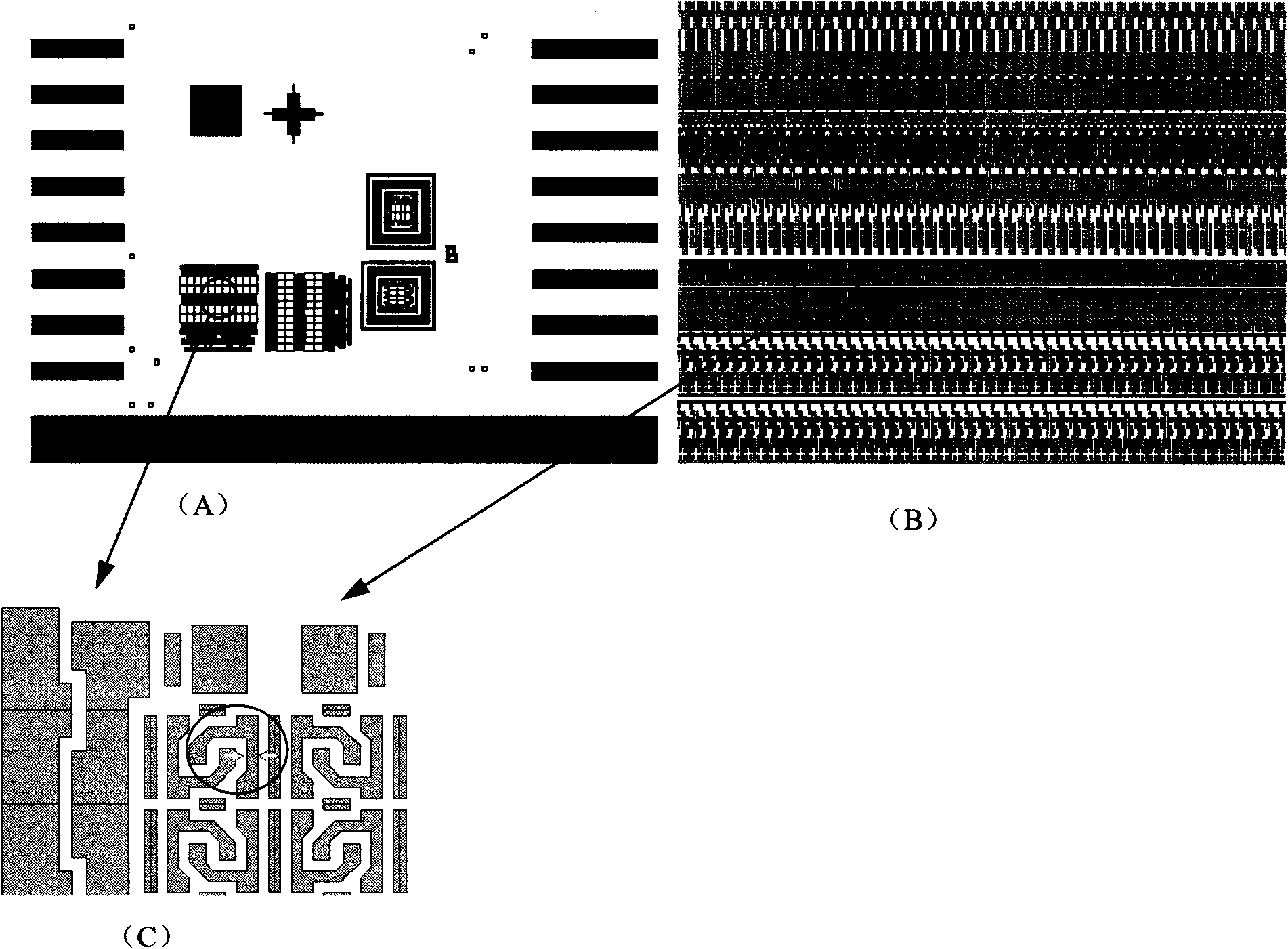
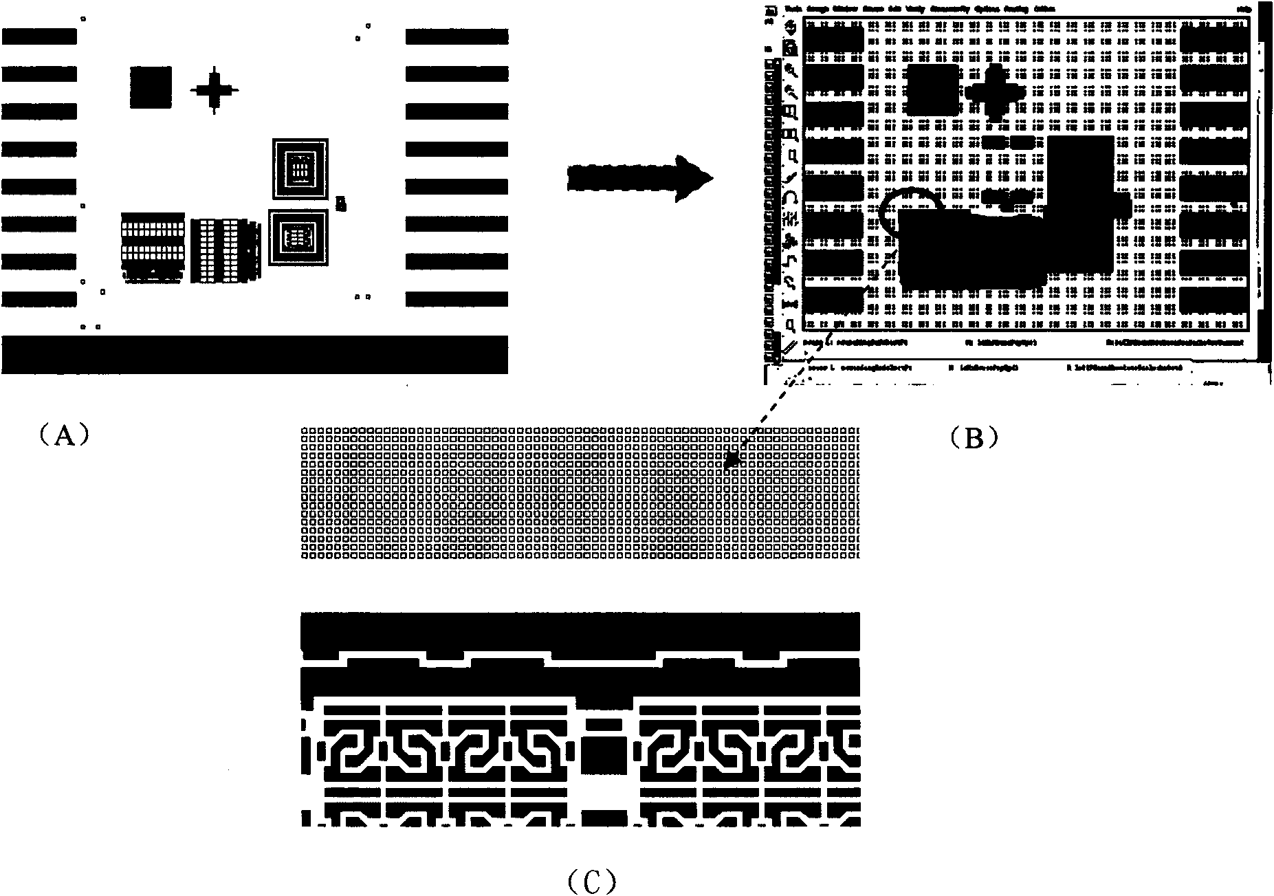
[0022] 1. In the photolithography process, before the mask plate is made, use OPC software or other related auxiliary software to insert auxiliary graphics in the layout according to certain rules. The general rule for inserting auxiliary graphics is: add multiple small-sized auxiliary graphics in the area where dummy patterns are not allowed to be inserted in the layout (chip design graphics). The "area where dummy graphics are inserted" usually refers to the dicing line or the open area far away from the working unit of the chip. Dummy graphics are allowed to be inserted, and small-sized auxiliary graphics are added in areas where dummy graphics are not allowed to be inserted to balance the difference in graphic density in different local areas. This small-sized au...


PUM


Abstract

The invention discloses a method for improving graphics critical dimension uniformity in a mask, which comprises the following steps in the technical process of photoetching: (1) adding a plurality of auxiliary graphics in areas in which virtual graphics are not permitted to be inserted in a domain before manufacturing the mask, thereby balancing difference of the graphics densities in different local areas; (2) manufacturing the mask in accordance with a revised domain which is added with the auxiliary graphics; and (3) forming chip graphics by the exposure of the photoetching technique. The invention can increase the graphic critical dimension in the chip unit on the mask and the uniformity of a section, thereby improving control of critical layers on a high wafer layer.

Description

technical field [0001] The invention relates to a semiconductor manufacturing process method, in particular to a semiconductor photolithography process method, in particular to a method for improving the uniformity of critical dimensions of a mask pattern. Background technique [0002] In the photolithography process, the critical dimension (CD, Critical Dimension, the smallest line width in the mask pattern) and the difference in cross-sectional shape on the mask will directly affect the uniformity control of the key pattern size of the photolithography process. Thereby affecting the realization of the electrical performance of the related chip unit. At the same time, the optimal process conditions of patterns in different local areas will be shifted, reducing the effective process window of lithography, thus making process control more difficult. Such as figure 1 and figure 2 as shown, figure 1 A and figure 1 B are different regions in a chip unit, and the pattern de...

Claims


Application Information

Patent Timeline
IPC IPC(8): G03F1/14G03F1/38
Inventor 何伟明魏芳
Owner SHANGHAI HUAHONG GRACE SEMICON MFG CORP
Why Eureka
Try Eureka