Eureka AIR delivers breakthrough ideas for toughest innovation challenges, trusted by R&D personnel around the world.

Method for preparing white light LED

A preparation process and LED chip technology, applied in the direction of electrical components, circuits, semiconductor devices, etc., can solve the problems of uneven coating of phosphor, expensive equipment, uneven light and color, etc., and achieve simple and mature screen printing process, improve Product consistency, the effect of improving production efficiency

Inactive Publication Date: 2010-11-24
上海科学院 +1
View PDF0 Cites 5 Cited by
  • Summary
  • Abstract
  • Description
  • Claims
  • Application Information

AI Technical Summary

Problems solved by technology

However, this technique has not been widely used due to the expensive equipment
Other manufacturers use phosphor powder dot coating to apply phosphor powder. Due to the effect of gravity and surface tension, the phosphor powder cannot be evenly coated, and the products will inevitably have different degrees of uneven light and color. Moreover, the output of white LEDs Limited by the speed of the phosphor dispensing process, it cannot be improved
Some manufacturers also use the groove structure to solve the uniformity of phosphor coating, but the inner surface of the groove loses seriously the light emitted from the side of the LED chip, and the luminous efficiency of the LED is not high.

Method used


Image

  • Method for preparing white light LED
  • Method for preparing white light LED
  • Method for preparing white light LED

Examples


Embodiment Construction

[0025] The technical solutions of the present invention will be further described below in conjunction with the drawings and embodiments.

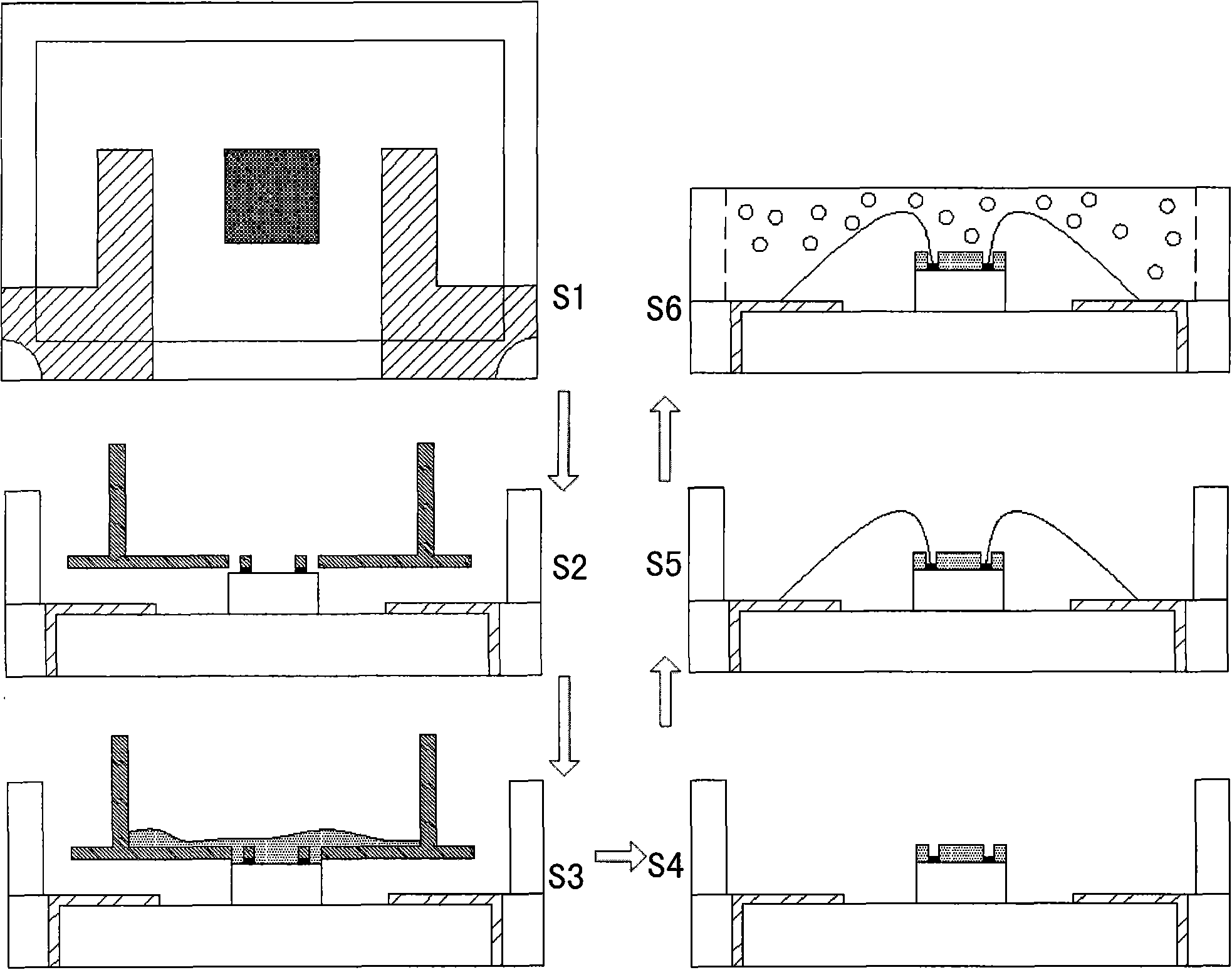
[0026] figure 1 The process flow of the embodiment of the manufacturing process method of the white light LED of the present invention is shown. See figure 1 , the preparation process of this embodiment is divided into 6 processes, which are crystal-bonding process S1, screen-on process S2, phosphor printing process S3, screen-removing and phosphor-baking process S4, and wire bonding process S5. And filling the silica gel step S6. Figure 2 to Figure 7 The six processes are shown respectively, and the six processes will be described below in conjunction with the accompanying drawings.

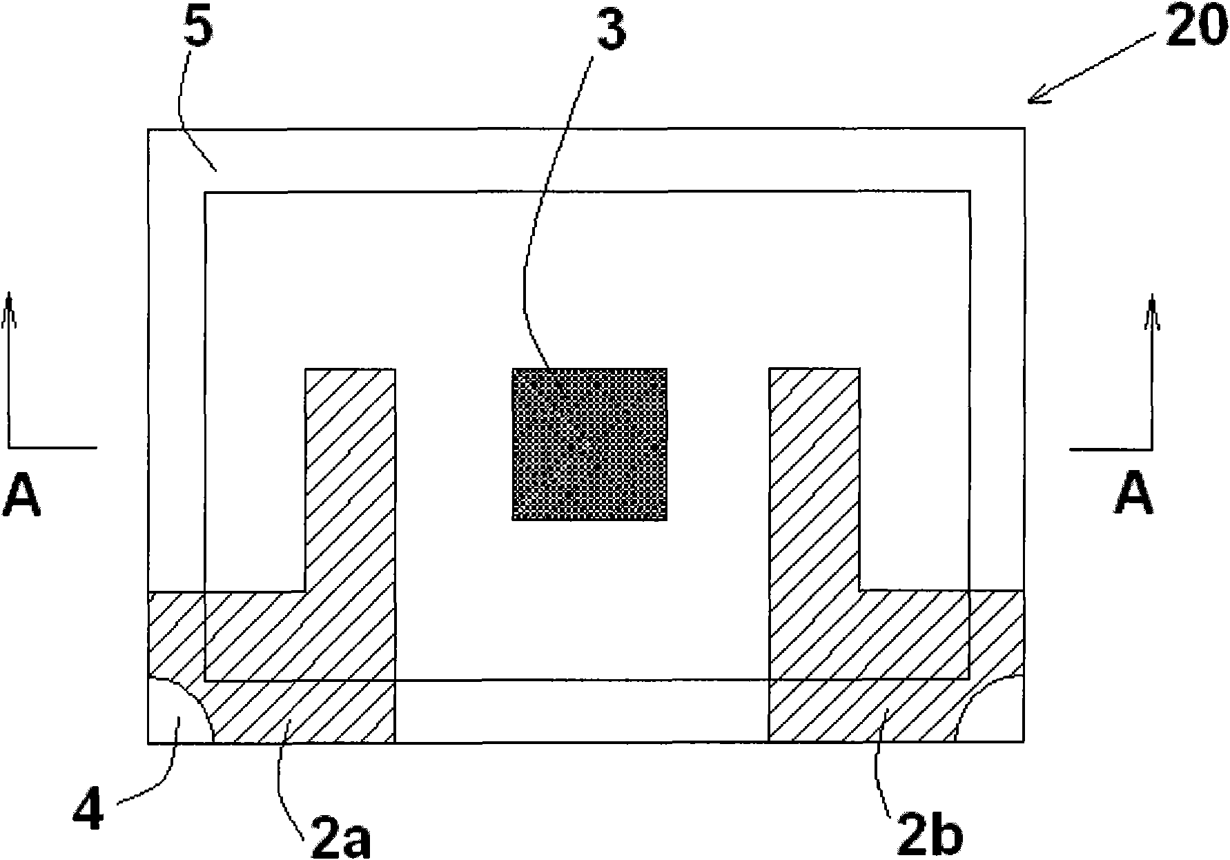
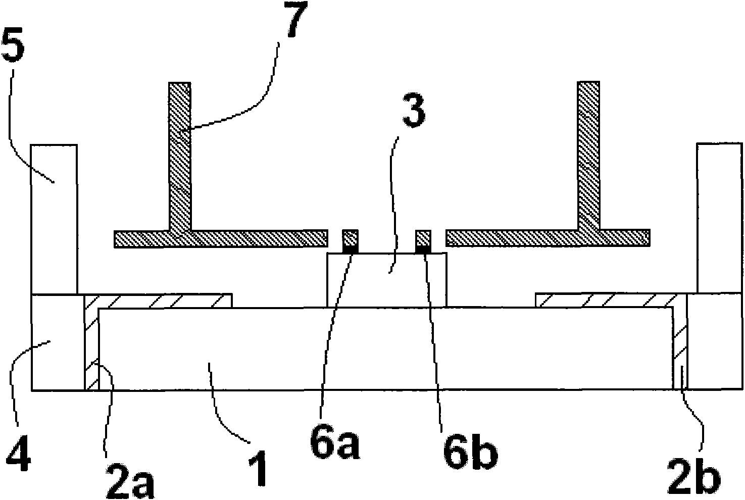
[0027] Die Bonding Process: Please refer to figure 2 , the blue LED chip 3 is fixed on the chip area by a chip bonding material, and two through holes 4 are provided on the side of the substrate, one of which corresponds to the positive electrode 2a of...


PUM

PropertyMeasurementUnit
Peak wavelengthaaaaaaaaaa

Abstract

The invention discloses a method for preparing a white light LED, which is suitable for preparing the white light LED connected with a lead frame in batch. The invention adopts the technical scheme that: the method comprises the following steps of: fixation: fixing a blue light LED chip on a chip area, providing two through holes corresponding to positive and negative electrodes of a substrate on the lateral surface of the substrate, and arranging a resin frame on the substrate; silk screen arrangement: forming the positive and negative electrodes of the substrate on the upper surface, extending the positive and negative electrodes to the inner surfaces of the through holes respectively, placing a silk screen at a position parallel to the surface of a chip, and making reserved holes of the silk screen correspond to patterns of the positive and negative electrodes of the chip; printing of fluorescent powder: printing the fluorescent powder on the surface of the chip by using a silk-screen printing process; removal of the silk screen and baking of the fluorescent powder: removing the silk screen, baking and curing the fluorescent powder, making the cured fluorescent powder coated on the surface of the chip, and exposing the positive and negative electrodes of the chip; lead bonding: connecting the positive electrodes of the chip and the substrate, and connecting the negative electrodes of the chip and the substrate; silica gel filling: filling silica gel into the resin frame, and baking and curing the silica gel to finish the preparation. The method is applied to the field of LED preparation.

Description

technical field [0001] The invention relates to an LED preparation process method, in particular to a white light LED preparation process method. Background technique [0002] LED is a semiconductor light-emitting device. The main light-emitting principle is that under the condition of forward voltage applied to the compound semiconductor material, electrons and holes in the active layer recombine to generate photons, and part of the recombination energy is emitted in the form of light energy. The visible light component can be Recognized by the human eye, resulting in usable light. Current LED chips can produce light of different colors depending on the material. AlGaAs can produce red light, InGaAlP can produce red, yellow, and yellow-green light, and InGaN can produce dark green and blue light. The three compound semiconductors can produce three primary colors, and a full-color light source can be produced by using different mixtures of the three colors. The light used...

Claims


Application Information

Patent Timeline
IPC IPC(8): H01L33/00
Inventor 周波
Owner 上海科学院
Why Eureka
Eureka Blog
Learn More