Novel MOS tube drive circuit for switch power supply

A technology of MOS tube and drive circuit, applied in the field of new MOS tube drive circuit, can solve the problems of increased cost, increased switching loss, high turn-on surge, etc., to achieve stable and reliable performance, reduce switching loss, and reduce turn-on surge. surge effect

Active Publication Date: 2010-11-24
GUANGDONG REAL DESIGN INTELLIGENT TECH
View PDF2 Cites 19 Cited by
  • Summary
  • Abstract
  • Description
  • Claims
  • Application Information

AI Technical Summary

Problems solved by technology

This method has the following problems: 1. Due to the existence of the gate-source junction capacitance of the MOS transistor, the MOS transistor cannot be turned off quickly, and the MOS transistor will temporarily enter the linear region, and the conduction internal resistance of the MOS transistor entering the linear region is very large. It will cause low efficiency of the MOS tube, increased switching loss, and severe heat generation; 2. Since the driving current provided by the control signal to the MOS tube rises rapidly (rising edge), it will cause a high turn-on surge, resulting in damage to the MOS tube , to a certain extent, it will also affect the EMC characteristics of the entire switching power supply
[0003] For problem 1, some people have made some improvements in the circuit, that is, a high-frequency diode is connected in antiparallel to the driving resistor to quickly discharge the gate charge and accelerate the turn-off of the MOS tube, but the improvement effect is not obvious; for problem 2, Some people directly solve this problem by adding a dedicated driver chip, but due to the high price of the chip, the cost will increase a lot, and there is a defect of high cost
The MOS tube drive circuit has the following disadvantages: 1. The MOS tube cannot be turned off quickly, the efficiency of the MOS tube is low, and the switching loss is large; 2. The overall circuit structure is complex and the cost is high

Method used


Image

  • Novel MOS tube drive circuit for switch power supply
  • Novel MOS tube drive circuit for switch power supply

Examples


specific Embodiment 1

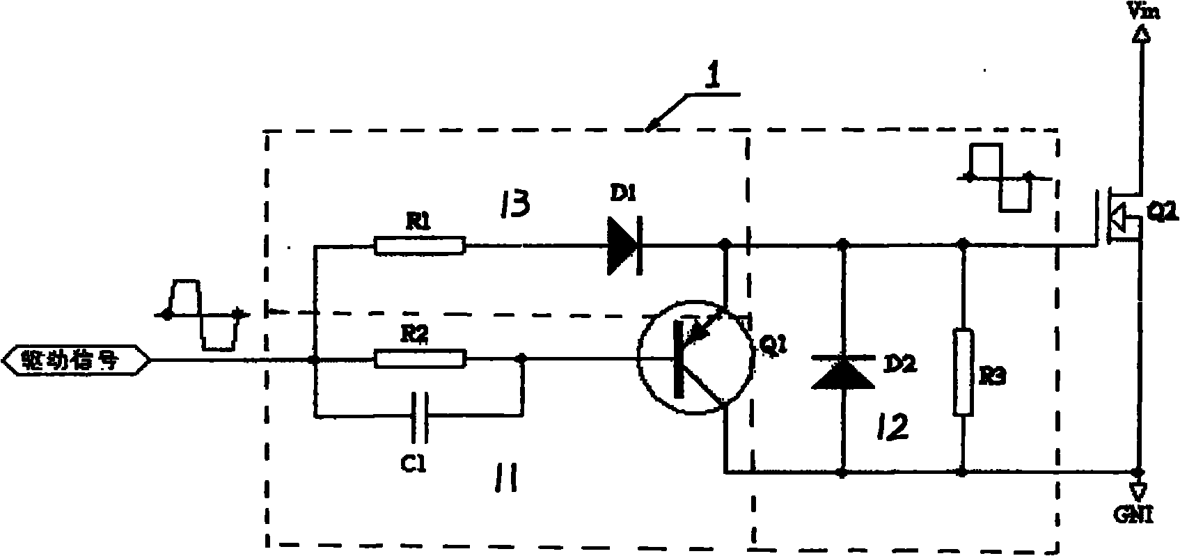
[0018] Reference figure 1 This embodiment includes a MOS transistor Q2 and a drive signal input terminal. A drive circuit 1 is provided at the connection between the control input terminal of the MOS transistor Q2 and the drive signal input terminal; the drive circuit 1 consists of a fast turn-off path 11 and a discharge path. 12 is connected with the surge prevention path 13; the quick turn-off path 11 and the surge prevention path 13 are connected in parallel and then connected across the control input terminal of the MOS transistor Q2 and the drive signal input terminal, and the discharge path 12 is connected across Between the gate and ground of the MOS tube.

[0019] In this embodiment, the driving circuit 1 is formed by connecting resistors R1 to R3, diodes D1 to D2, a filter capacitor C1 and a transistor Q1; the resistor R2 is connected in parallel with the filter capacitor C1 and then connected to the base of the transistor Q1 to form a fast turn-off path 11. The resista...

specific Embodiment 2

[0025] The specific embodiment 2 of the present invention is characterized in that: the driving tube Q1 is composed of a MOS tube, the gate of the MOS tube is connected to the output terminal of the fast turn-off path 11, the source is connected to the ground terminal, and the drain is connected to the anti-wave The output end of the surge path 13 is connected; that is, the resistor R2 and the filter capacitor C1 are connected in parallel to the gate of the MOS tube to form a fast turn-off path 11, and the resistor R1 and diode D1 are connected in series to the gate of the MOS tube to form a fast turn-off path 11 , The resistor R1 and the diode D1 are connected in series with the drain of the MOS transistor to form a surge prevention path 13, and the discharge resistor R3 is connected across the gate of the MOS switch Q2 and the ground to form a discharge path 12. The MOS switch Q2 The source of the MOS tube and the collector of the MOS tube are grounded.

specific Embodiment 3

[0026] The characteristic of the specific embodiment 3 of the present invention is: omit figure 1 The voltage limiting diode D2 shown is the same as the specific embodiment 1 or specific embodiment 2.


PUM


Abstract

The invention relates to a novel MOS tube drive circuit for a switch power supply, which comprises a MOS switch tube Q2 and a driving signal input terminal. The MOS tube drive circuit is characterized in that: a drive circuit (1) is arranged at the joint of a control input terminal of the MOS switch tube Q2 and the driving signal input terminal; the drive circuit (1) is formed by connecting a quick turn-off access (11), a discharging access (12) and a surging impact prevention access (13); the quick turn-off access (11) is connected in parallel with the surging impact prevention access (13) and then spans between the control input terminal of the MOS switch tube Q2 and the driving signal input terminal; and the discharging access (12) spans between a grid and an earth terminal of the MOS switch tube Q2. The MOS tube drive circuit can accelerate the turn-off of the MOS tube, control the ascending speed of driving current of the MOS tube effectively and improve the EMC characteristic ofthe integral switch power supply, and has the advantages of simple circuit, stable and reliable performance, easy realization and low cost.

Description

Technical field [0001] The present invention relates to the technical field of switching power supply drive circuits, in particular to a novel MOS tube drive circuit of a switching power supply. It belongs to the technical field of electronic switching power supplies. Background technique [0002] At present, most switching power supply circuits use MOS transistor drive circuits. A drive signal with an adjustable duty cycle is applied to the gate of the MOS transistor, and the output of the switching power supply is realized by controlling the on and off time of the MOS transistor. Effective control of voltage. The MOS drive circuit in the prior art generally adopts the following method: the control signal output from the control chip or generated by the oscillation circuit is connected to the gate of the MOS transistor through a drive resistor to realize on-off control of the MOS transistor. This method has the following problems: 1. Due to the existence of the gate-source jun...

Claims


Application Information

Patent Timeline
IPC IPC(8): H03K17/687H03K17/04
Inventor 汪军郑魏周治国
Owner GUANGDONG REAL DESIGN INTELLIGENT TECH
Why Eureka
Try Eureka