

Method for cleaning wafer after chemical mechanical polishing
A chemical machinery and wafer cleaning technology, applied in chemical instruments and methods, cleaning methods using tools, cleaning methods using liquids, etc. Stability and other issues to achieve the effect of improving reliability and stability, preventing excessive corrosion, and avoiding pit defects
- Summary
- Abstract
- Description
- Claims
- Application Information
AI Technical Summary
Problems solved by technology
Method used
Image

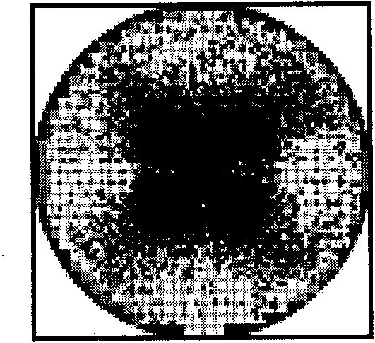
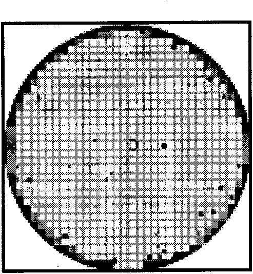
Examples
Embodiment Construction
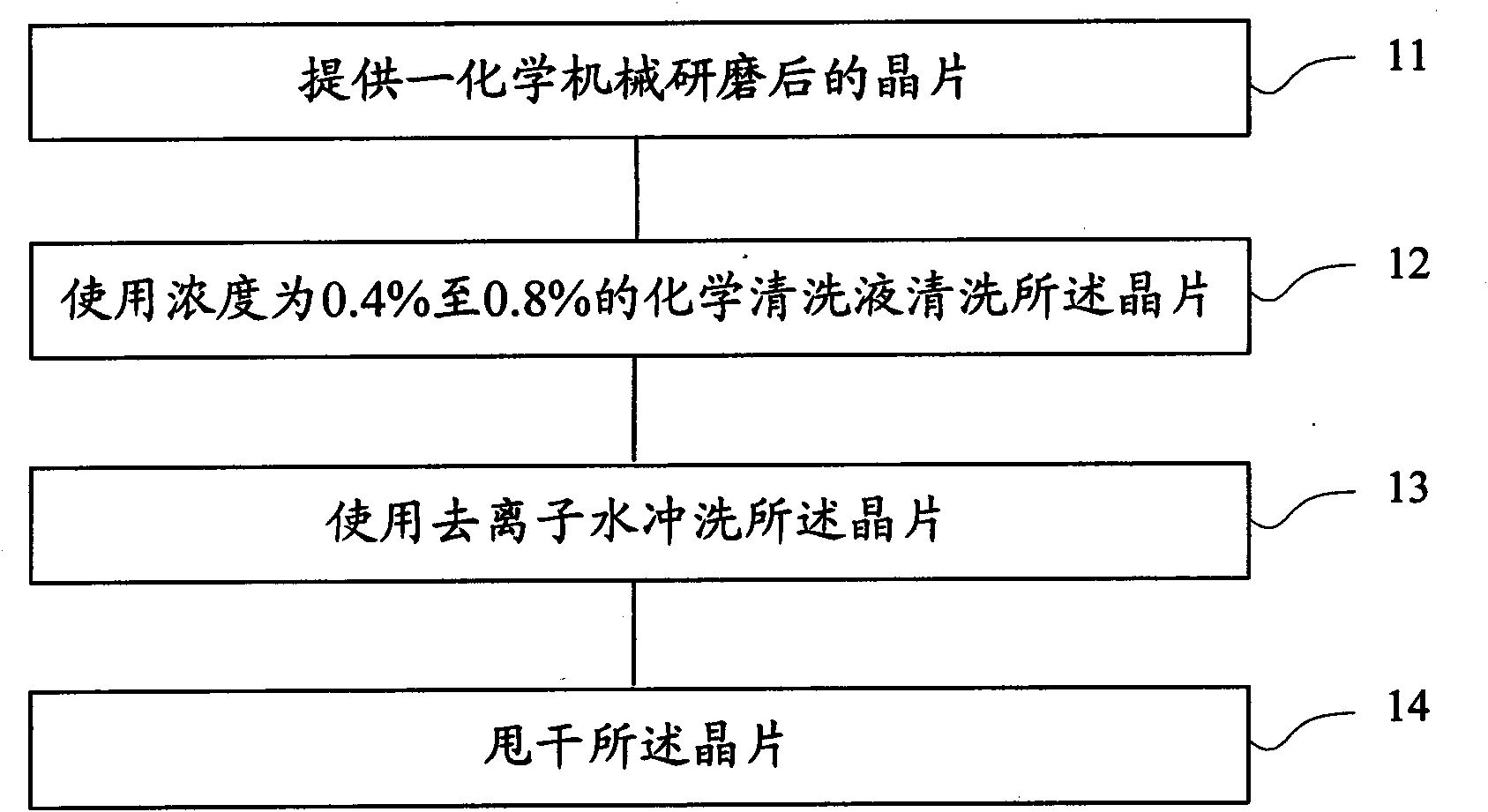
[0016] In order to make the purpose and features of the present invention more comprehensible, the specific implementation manners of the present invention will be further described below in conjunction with the accompanying drawings.
[0017] In the field of integrated circuit manufacturing, copper has replaced aluminum to become the mainstream interconnection technology in ultra large scale integrated circuit (Ultra Large Scale Integrated Circuit, USLI) manufacturing. Generally speaking, the copper process dual damascene process usually includes the following steps: first, deposit an insulating layer with a certain thickness on the wafer with semiconductor devices, then etch the insulating layer to form trenches for the damascene process, and then, through electroplating The process fills the trench with metal copper, and finally uses chemical mechanical polishing to planarize the surface of the wafer.
[0018] At present, the industry usually uses a chemical cleaning soluti...
PUM
 Abstract
Description
Claims
Application Information