Process for forming side electrode of chip concave type electrode network resistor

A side electrode, concave technology, used in resistors, resistance manufacturing, coating resistance materials, etc., can solve the problems of air flow end-face electrode filling holes cannot be guaranteed to be consistent, poor customer satisfaction, and inconsistent filling holes. Achieve the effect of overcoming the incomplete connection to form effective side electrodes, enhancing product market competitiveness and reducing production costs

Active Publication Date: 2010-12-15
UNIROYAL ELECTRONICS IND
View PDF0 Cites 6 Cited by
  • Summary
  • Abstract
  • Description
  • Claims
  • Application Information

AI Technical Summary

Problems solved by technology

[0006] However, when forming the side electrodes of the SMD concave electrode network resistor, the side electrodes are formed by a combination of front printed filling holes and back printed filling holes. During the manufacturing process, due to the warping problem of the substrate, the vacuum of the filling holes will be inconsistent. In addition, the position of the substrate perforation is different, so that the path of the airflow is inconsistent, and the depth of the end electrode filling hole cannot be guaranteed to be consistent. In this way, the upper and lower parts of the side electrodes formed by the upper and lower filling holes will inevitably appear unable to connect. Or in the case of incomplete connection, there will be certain quality hidden dangers when the product is used on the client side, resulting in an increase in defects in the production process and a decrease in customer satisfaction

Method used


Image

  • Process for forming side electrode of chip concave type electrode network resistor
  • Process for forming side electrode of chip concave type electrode network resistor
  • Process for forming side electrode of chip concave type electrode network resistor

Examples


Embodiment

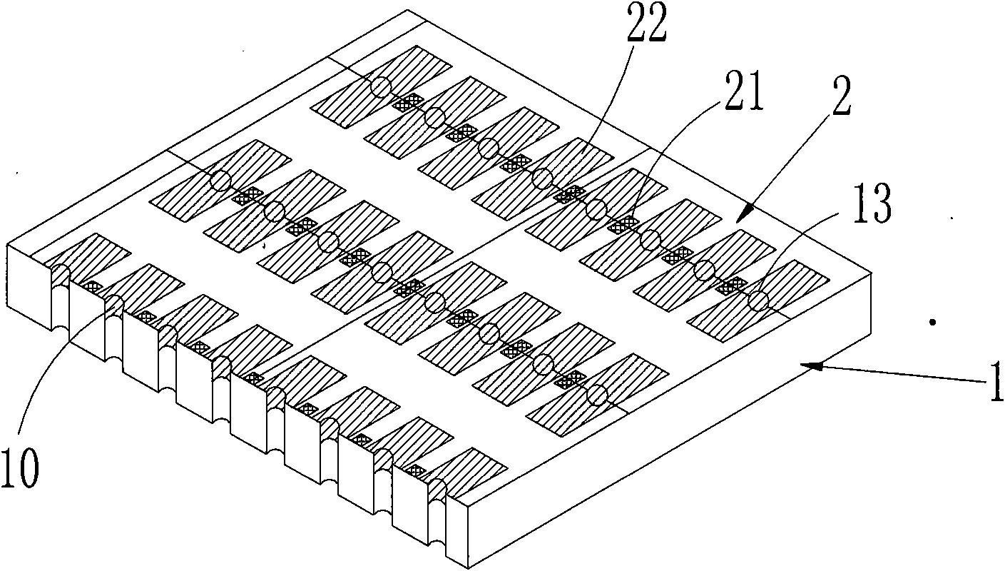
[0020] Embodiment: A side electrode formation process of patch concave electrode network resistance, based on the use direction, after printing the front electrode 22 on the upper surface 2 of the insulating substrate 1 corresponding to the perforation 13, each perforation 13 is filled. Thereby forming the side electrode conduction layer 10 on the upper part of each perforation 13 hole walls, the formation process of the side electrodes is as follows:

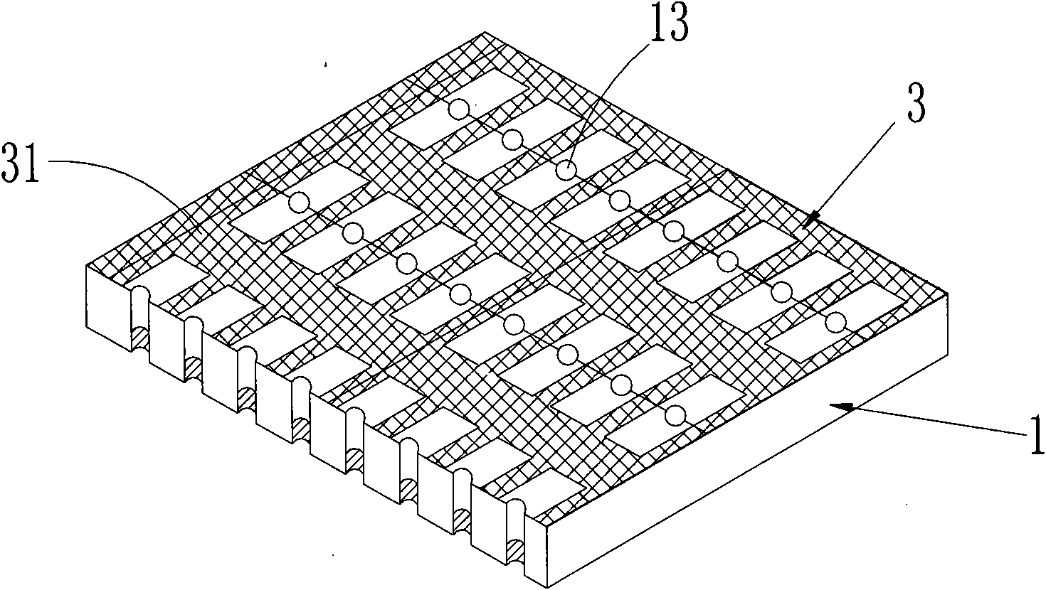
[0021] a. Print and form a mask layer 31 on the part of the lower surface 3 of the insulating substrate 1 corresponding to the position of the upper surface of the front electrode 22, and dry it;

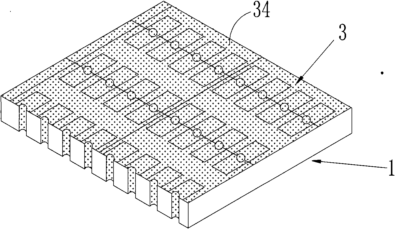
[0022] b. The lower surface 3 of the insulating substrate is sputtered, and the sputtering layer 34 is formed on the position of the mask layer 31, the hole wall of the perforation 13, and the lower surface 3 of the insulating substrate corresponding to the front electrode 22 on the upper surface (ie Sputtering is performed on the en...


PUM


Abstract

The invention discloses a process for forming a side electrode of a chip concave type electrode network resistor. The process comprises the following steps of: forming a side electrode conduction layer which is the upper part of the side electrode in the prior art in a hole filling way after printing a front electrode; forming a back electrode and a through hole wall sputtering layer in the way of film-shaped sputtering by mask sputtering; and completely covering the side electrode conduction layer with the through hole wall sputtering layer to form an effective side electrode. The process overcomes the defect of the prior art that the front electrode and the back electrode of an resistor can not be completely connected to form a conductive side electrode since the buckling of an insulation substrate is not consistent with a hole filling path, thereby greatly reducing hidden quality dangers; in addition, since a base metal alloy material is used for sputtering the sputtering layers and cost and consumption are both lower, the production cost is effectively lowered and the market competitiveness of the products is enhanced.

Description

technical field [0001] The invention relates to a method for manufacturing a resistor, in particular to a process for forming a side electrode of a patch concave electrode network resistor. Background technique [0002] SMD concave electrode network resistors can be widely used in various electrical appliances, personal data storage, mobile phones and other communication products due to their small size, high power, dense arrangement, and easy placement, and promote the further miniaturization of this type of electronic products At the same time, because the electrode spacing is relatively small, the internal stress of the electrode installation is reduced, and the problems such as substrate fracture are greatly reduced. [0003] The side electrode formation process of a typical patch concave electrode network resistor is: [0004] 1. Use screen printing to form the front electrode on the front of the large insulating substrate, and use special filling equipment to form the...

Claims


Application Information

Patent Timeline
Patent Type & Authority Applications(China)
IPC IPC(8): H01C17/28H01C17/12H01C17/065
Inventor 王毅冯会军张军会刘冰芝彭荣根张翔
Owner UNIROYAL ELECTRONICS IND
Why Eureka
Try Eureka