Wafer carrying device
A wafer carrying and height adjustment device technology, which is applied in the direction of electrical components, semiconductor/solid-state device manufacturing, circuits, etc., can solve the problems of affecting the quality of the film, the height of the wafer plate can not be adjusted in real time, and reduce the use efficiency, so as to broaden the use Range, efficiency gains, and time-consuming effects
- Summary
- Abstract
- Description
- Claims
- Application Information
AI Technical Summary
Problems solved by technology
Method used
Image
Examples
Embodiment 1
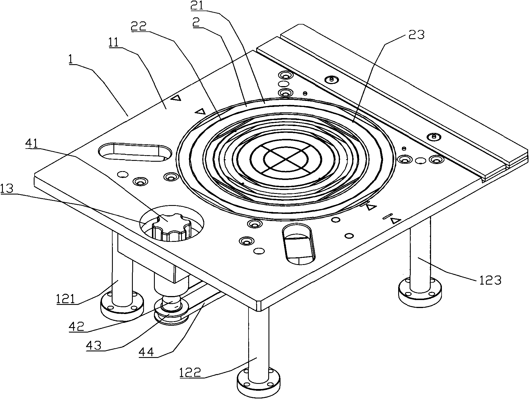
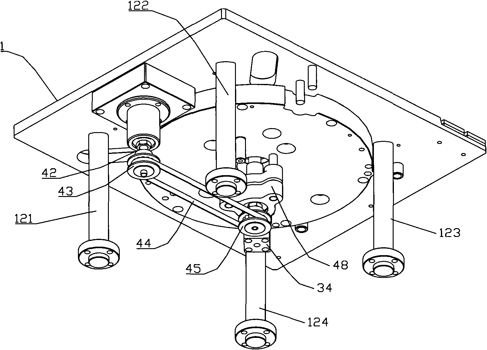
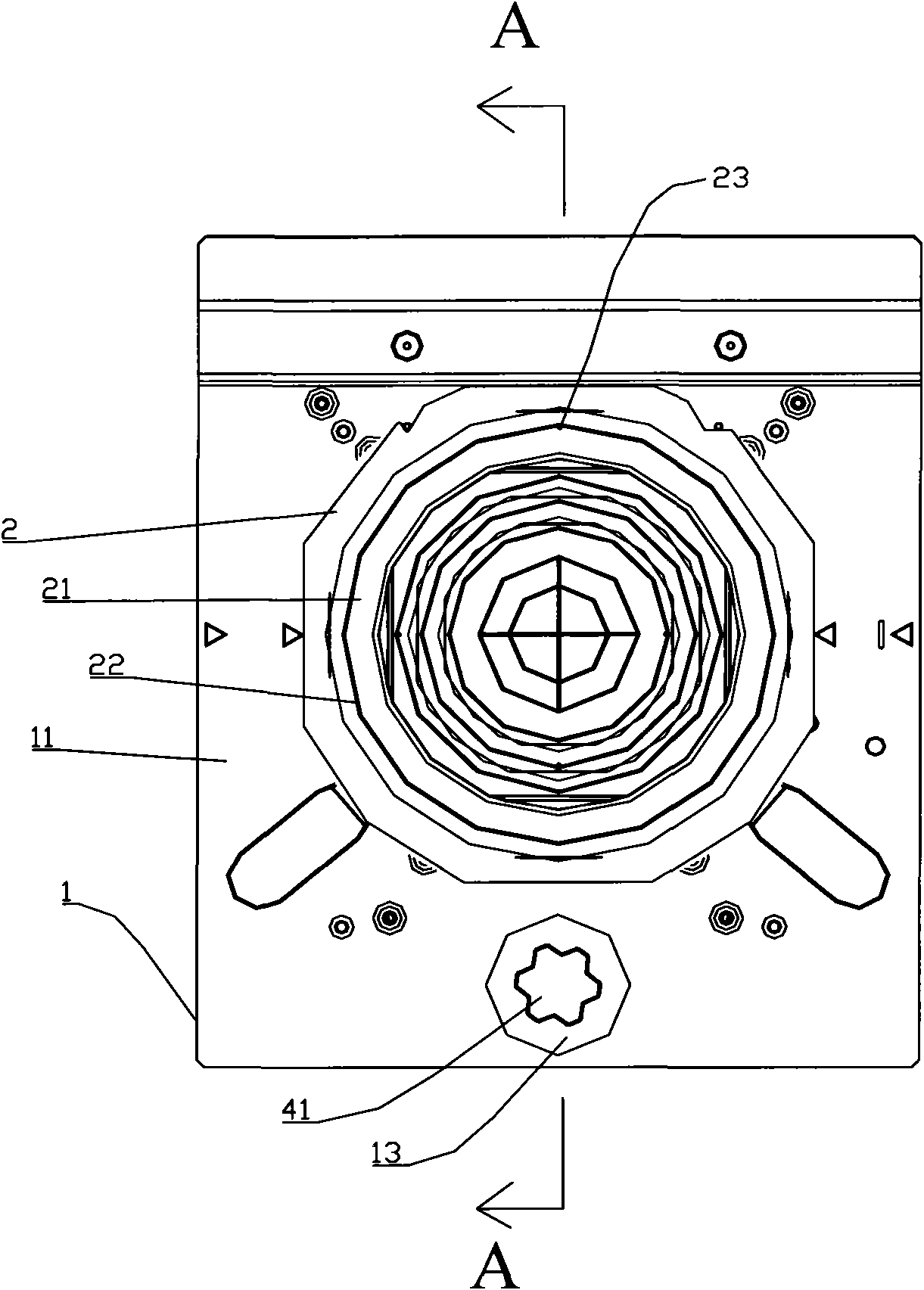
[0041] Such as figure 1 , figure 2 and image 3 As shown, the wafer carrying device includes a base 1, and the upper surface 11 of the base 1 is provided with a first groove (not shown in the figure). Four seat legs ( 121 , 122 , 123 , 124 ) are installed on the lower surface of the base 1 for supporting the base 1 . The upper surface 11 of the base 1 is provided with a third groove 13 .
[0042] The first platform 2 is movably installed in the first groove. The upper surface 21 of the first platen 2 is provided with a first vacuum groove 22 . There are more than two first vacuum grooves 22 (only one is marked in the figure), and each first vacuum groove 22 is arranged around the upper surface 21 of the first platform 2 . Each first vacuum groove 22 communicates with a first through hole 23 provided on the first platform 2 . During actual use, the wafer is placed on the upper surface 21 of the first platen 2, covers the first vacuum chamber 22, makes the first through h...
Embodiment 2
[0048] Such as Figure 6 , Figure 7 and Figure 8 As shown, the wafer carrying device includes a base 1, and the upper surface 11 of the base 1 is provided with a first groove (not shown in the figure). Four seat legs ( 121 , 122 , 123 , 124 ) are installed on the lower surface of the base 1 for supporting the base 1 . The upper surface 11 of the base 1 is provided with a third groove 13 .
[0049] The first platform 2 is movably installed in the first groove. The upper surface 21 of the first platen 2 is provided with a first vacuum groove 22 . There are more than two first vacuum grooves 22 (only one is marked in the figure), and each first vacuum groove 22 is arranged around the upper surface 21 of the first platform 2 . Each first vacuum groove 22 communicates with a first through hole 23 provided on the first platform 2 . In actual use, the wafer is placed on the upper surface 21 of the first platform 2, and the first vacuum chamber 22 is covered, so that the first...
PUM
 Abstract
Description
Claims
Application Information


