SOI (Silicon on Insulator) variable buried oxide layer thickness device and preparation method thereof

A buried oxide layer and device technology, applied in semiconductor/solid-state device manufacturing, semiconductor devices, electric solid-state devices, etc., can solve problems such as the inability to make full use of the drift region, and achieve the effect of uniform surface electric field and improved breakdown performance

Active Publication Date: 2010-12-15
SICHUAN CHANGHONG ELECTRIC CO LTD
View PDF6 Cites 15 Cited by
  • Summary
  • Abstract
  • Description
  • Claims
  • Application Information

AI Technical Summary

Problems solved by technology

[0003] The purpose of the present invention is to overcome the shortcoming that the electric field distribution presents high at both ends and low in the middle when the current SOILDMOS device breaks down, which cannot make full use of the drift region, and provides a SOI variable buried oxide layer thickness device and its preparation method

Method used


Image

  • SOI (Silicon on Insulator) variable buried oxide layer thickness device and preparation method thereof
  • SOI (Silicon on Insulator) variable buried oxide layer thickness device and preparation method thereof
  • SOI (Silicon on Insulator) variable buried oxide layer thickness device and preparation method thereof

Examples


Embodiment

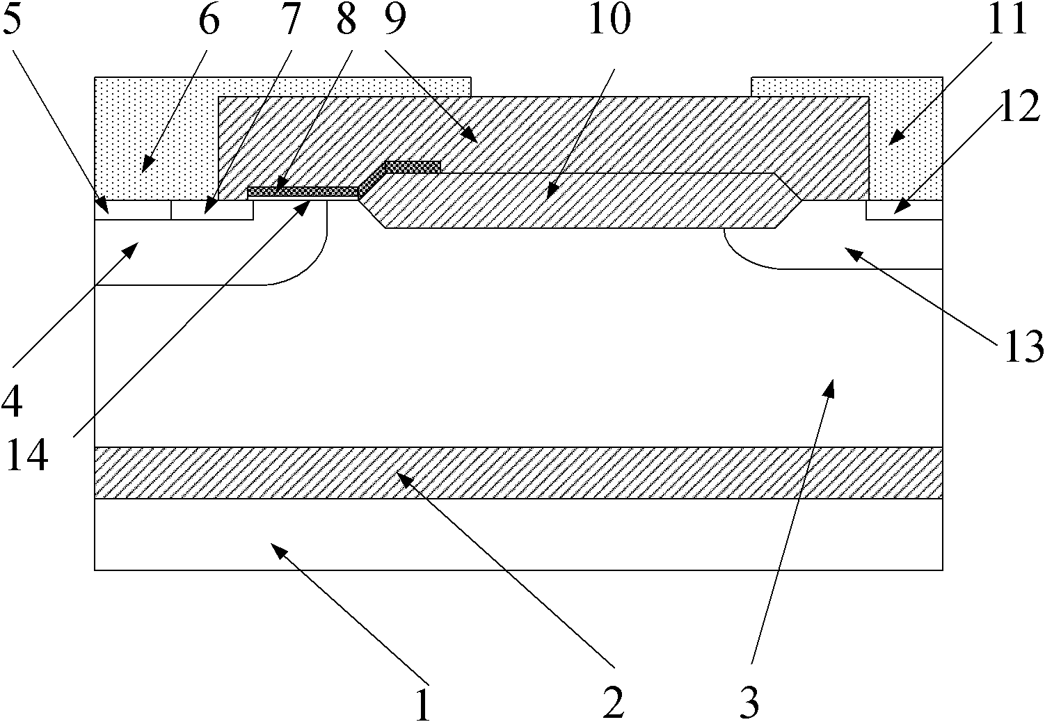
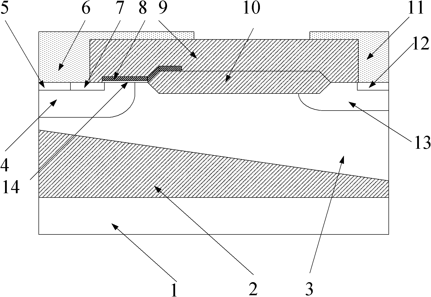
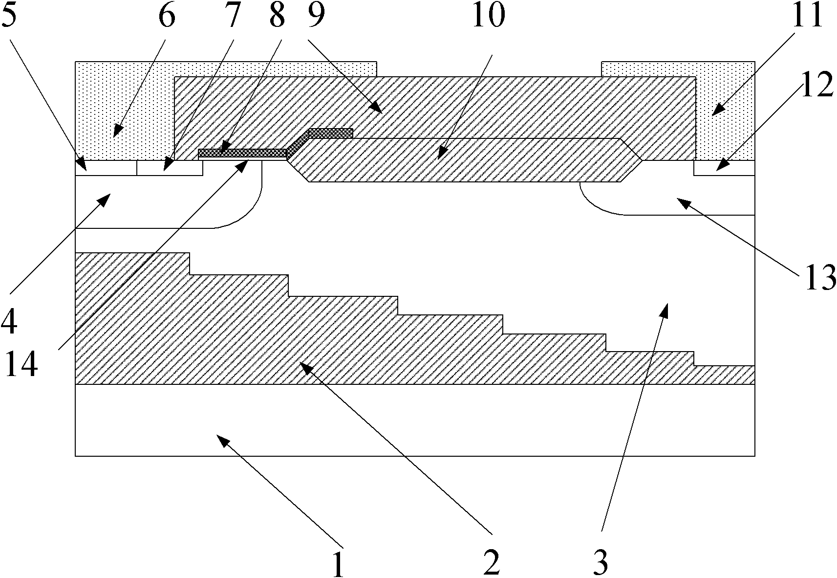
[0031] In the SOI variable buried oxide layer thickness device in this example, the thickness variation of the buried oxide layer can be continuous or stepped. The cross-sectional view of the SOILDMOS device when the buried oxide layer is continuously changing is as follows figure 2 , the cross-sectional view of the SOILDMOS device when the buried oxide layer changes in steps is as follows image 3 , the breakdown characteristic curves of conventional SOILDMOS devices and the SOILDMOS devices of this embodiment are as follows Figure 4 , the surface field distribution characteristic curves of the conventional SOILDMOS device and the SOILDMOS device of this embodiment are as follows Figure 5 , the conventional SOI LDMOS device and the SOILDMOS device of this embodiment have breakdown voltage and drift region concentration variation curves as shown in Image 6 .

[0032] The thickness of the buried oxide layer of the SOI variable buried oxide layer thickness device gradually...


PUM


Abstract

The invention relates to an SOI (Silicon on Insulator) technology, which solves the problems of uneven distribution of electric field with both high ends and low middle during breakdown and insufficient utilization of a drift area of a traditional SOILDMOS (Silicon on Insulator Lateral Double Diffused Metal Oxide Semiconductor) device. The invention provides an SOI variable buried oxide layer thickness device and a preparation method thereof. in the technical scheme, the SOI variable buried oxide layer thickness device comprises a source electrode, a drain electrode, a buried oxide layer and n-shaped top SOI impurity material layer, and is characterized in that the thickness of the buried oxide layer is gradually reduced from the source electrode to the drain electrode; and the thickness of the n-shaped top SOI impurity material layer is gradually increased from the source electrode to the drain electrode. The invention has the advantage of largely enhanced breakdown performance, and is suitable for the SOILDMOS device.

Description

technical field [0001] The invention relates to SOI technology, in particular to a SOILDMOS device and a preparation method thereof. Background technique [0002] SOI technology uses a relatively simple dielectric isolation process to make SOI devices have the advantages of small parasitic effects, fast speed, low power consumption, high integration, and strong radiation resistance. In SOI technology, LDMOS devices are integrated, that is, SOILDMOS devices. Complete dielectric isolation between active devices and material substrates and other high and low voltage devices is beneficial to avoid latch-up effects of LDMOS devices, and high voltage devices on SOI can be monolithically integrated with low voltage logic drive circuits; cross-sectional view of conventional SOILDMOS devices Such as figure 1 , where 1 is the p-type substrate, 2 is the buried oxide layer, 3 is the n-type top layer SOI impurity material, 4 is the source p well, which is used as the LDMOS channel regio...

Claims


Application Information

Patent Timeline
Patent Type & Authority Applications(China)
IPC IPC(8): H01L29/78H01L27/12H01L21/336H01L21/762
CPCH01L29/7824
Inventor 梁涛罗波
Owner SICHUAN CHANGHONG ELECTRIC CO LTD
Why Eureka
Try Eureka