Ultrahigh frequency band near field RFID reader-writer antenna
A technology of ultra-high frequency bands and readers, which is applied in the direction of antennas, antenna supports/mounting devices, electrical components, etc., can solve problems such as narrow bandwidth, and achieve the effect of strong magnetic field, lower precision requirements, and frequency bandwidth
- Summary
- Abstract
- Description
- Claims
- Application Information
AI Technical Summary
Problems solved by technology
Method used
Image
Examples
Embodiment 1
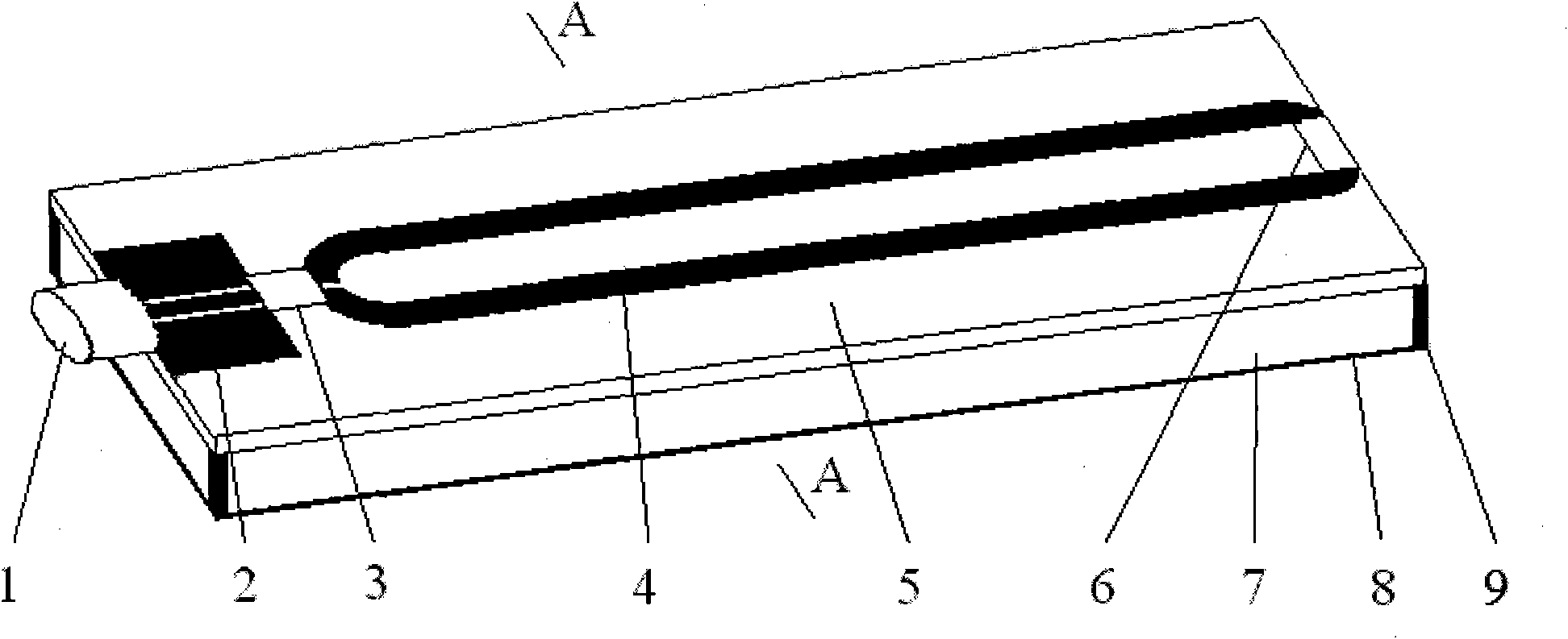
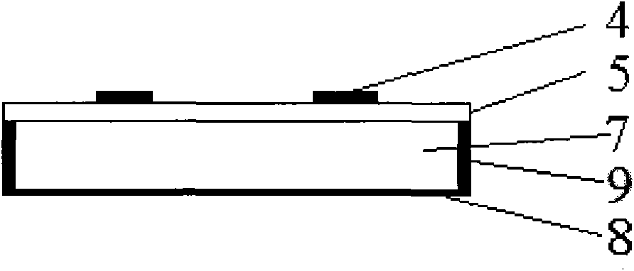
[0015] The length and width of the PCB substrate 5 and the metal floor 8 are 110mm and 50mm respectively; the PCB substrate 5 adopts FR4 dielectric board with a thickness of 1.5mm and a relative dielectric constant of 4.4; the thickness of the air layer 7 is 5mm.
[0016] Select the center conduction strip width and the slot width of the coplanar waveguide 2 so that its characteristic impedance is 50Ω, so as to match with the coaxial connector 1 . A balun with an impedance ratio of 1:4 is used. The port impedance of the balun 3 on the side of the coplanar waveguide 2 is 50Ω, and the port impedance on the side of the coplanar stripline 4 is 200Ω. The width of the conduction band of the coplanar stripline 4 is selected as 5mm and the distance between the conduction bands is 10mm, so that the characteristic impedance thereof is 200Ω. The impedance of the resistor 6 is 200Ω, which matches the characteristic impedance of the coplanar stripline 4 .
[0017] From the coaxial connec...
Embodiment 2
[0023] Both the reduction of the characteristic impedance of the coplanar strip line 4 and the increase of the thickness of the air layer 7 will increase the magnetic field strength and further extend the operating distance of the antenna.
[0024] The length and width of the PCB substrate 5 and the metal floor 8 are 110mm and 80mm respectively; the PCB substrate 5 is made of FR4 dielectric board with a thickness of 1.5mm and a relative dielectric constant of 4.4; the thickness of the air layer 7 is 10mm.
[0025] Select the center conduction strip width and the slot width of the coplanar waveguide 2 so that its characteristic impedance is 50Ω, so as to match with the coaxial connector 1 . A balun with a 1:2 impedance ratio is used. The port impedance of the balun 3 on the side of the coplanar waveguide 2 is 50Ω, and the port impedance on the side of the coplanar stripline 4 is 100Ω. The width of the conduction band of the coplanar stripline 4 is selected as 35mm and the dist...
PUM
 Abstract
Description
Claims
Application Information


