
Organic light-emitting device

An organic light-emitting device and organic light-emitting layer technology, applied in photovoltaic power generation and other directions, can solve problems such as application scope limitation, and achieve the effect of expanding applicable fields, avoiding energy waste and environmental pollution, and having a simple structure.

Inactive Publication Date: 2010-12-22
SHANGHAI HONGYUAN LIGHTING & ELECTRICAL EQUIP
View PDF0 Cites 0 Cited by
  • Summary
  • Abstract
  • Description
  • Claims
  • Application Information

AI Technical Summary

Problems solved by technology

[0008] The present invention aims to solve the technical problems in the prior art that the organic light emitting diode element is only applied to the display and is not combined with solar energy, so that its application range is limited.

Method used


Image

  • Organic light-emitting device
  • Organic light-emitting device
  • Organic light-emitting device

Examples


Embodiment 1

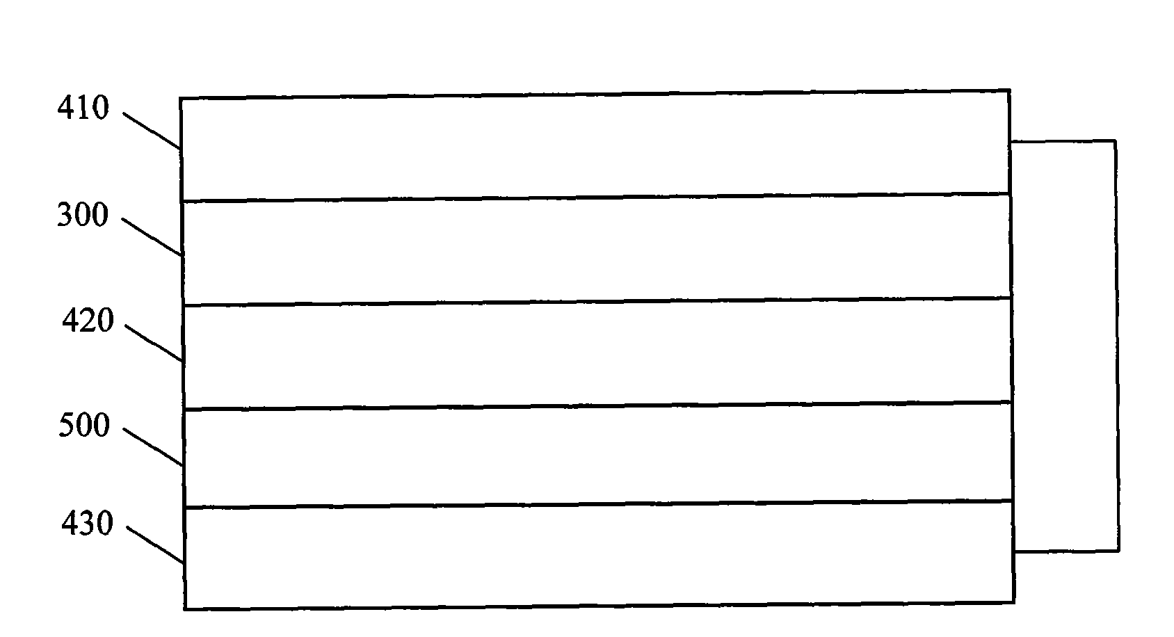
[0027] See Figure 3A , which is a schematic structural diagram of an organic light-emitting device provided in Embodiment 1 of the present invention.

[0028] As shown in the figure, the organic light-emitting device includes: a first electrode layer 410, an organic light-emitting layer 300, a second electrode layer 420, a solar semiconductor composite layer 500, and a third electrode layer 430 stacked in sequence, wherein the first The electrode layer 410 is electrically connected to the third electrode layer 430 .

[0029] Usually, the polarity of the first electrode layer 410 is the same as that of the third electrode layer 430 and opposite to that of the second electrode layer 420 , thereby forming a common electrode structure of the organic light emitting layer 300 and the solar semiconductor composite layer 500 . In this embodiment, the first electrode layer 410 and the third electrode layer 430 are the anode layer, and the second electrode layer 420 is the cathode lay...

Embodiment 2

[0037] See Figure 4 , which is a schematic structural diagram of an organic light-emitting device provided in Embodiment 2 of the present invention.

[0038]In this embodiment, the organic light-emitting device includes: a first electrode layer 410, an organic light-emitting layer 300, a second electrode layer 420, a solar semiconductor composite layer 500, and a third electrode layer 430 stacked in sequence, wherein the first electrode The layer 410 is electrically connected to the third electrode layer 430 . It also includes: a storage battery 600, which includes a first electrode 610 and a second electrode 620; the first electrode 610 is electrically connected to the first electrode layer 410 and the third electrode layer 430; the second electrode 620 is connected to the The second electrode layer 420 is electrically connected.

[0039] Usually, the polarity of the first electrode layer 410 is the same as that of the third electrode layer 430 and opposite to that of the ...


PUM


Abstract

The invention discloses an organic light-emitting device which comprises a first electrode layer, an organic light-emitting layer, a second electrode layer, a solar semiconductor compound layer and a third electrode layer which are sequentially stacked, wherein the first electrode layer is electrically connected with the third electrode layer. The device utilizes an organic light-emitting diode device, is applied in the field of lighting and is further combined with the solar energy technology, thereby using clean energy in lighting, achieving the good lighting effect, simultaneously saving the energy and avoiding the waste of the energy and the environmental pollution; furthermore, the device has simple structure, adopts the thin design and is applicable to various fields.

Description

technical field [0001] The invention relates to the technical field of display and illumination, in particular to an organic light-emitting device. Background technique [0002] Organic Light Emitting Diode (OLED) is a brand-new display technology whose display quality is comparable to Thin Film Transistor Active Liquid Crystal Display (TFT LCD), and the price is far lower than it, it will challenge the widely used LCD technology . Since 1987, C.W.Tang and VanSlyke reported that the brightness exceeds 1000cd / m when working at low voltage 2 Since the double-layer organic thin-film light-emitting device, OLED has increasingly become a hot spot in international research because of its remarkable advantages in flat-panel displays, such as high luminous brightness, rich colors, low-voltage DC drive, and simple manufacturing process. In less than 20 years, OLED has entered the stage of industrialization from research. [0003] The basic structure of an OLED display is a thin, t...

Claims


Application Information

Patent Timeline
Patent Type & Authority Applications(China)
IPC IPC(8): H01L51/50H01L31/042
CPCY02E10/50
Inventor 郭超李维德陈育明
Owner SHANGHAI HONGYUAN LIGHTING & ELECTRICAL EQUIP
Features
  • Generate Ideas
  • Intellectual Property
  • Life Sciences
  • Materials
  • Tech Scout
  • Unparalleled Data Quality
  • Higher Quality Content
  • 60% Fewer Hallucinations
Learn More