

Printed circuit board
一种印刷电路板、集成电路的技术,应用在印刷电路、印刷电路、印刷电路制造等方向,能够解决损坏集成电路本身等问题
- Summary
- Abstract
- Description
- Claims
- Application Information
AI Technical Summary
Problems solved by technology
Method used
Image

Examples
Embodiment Construction
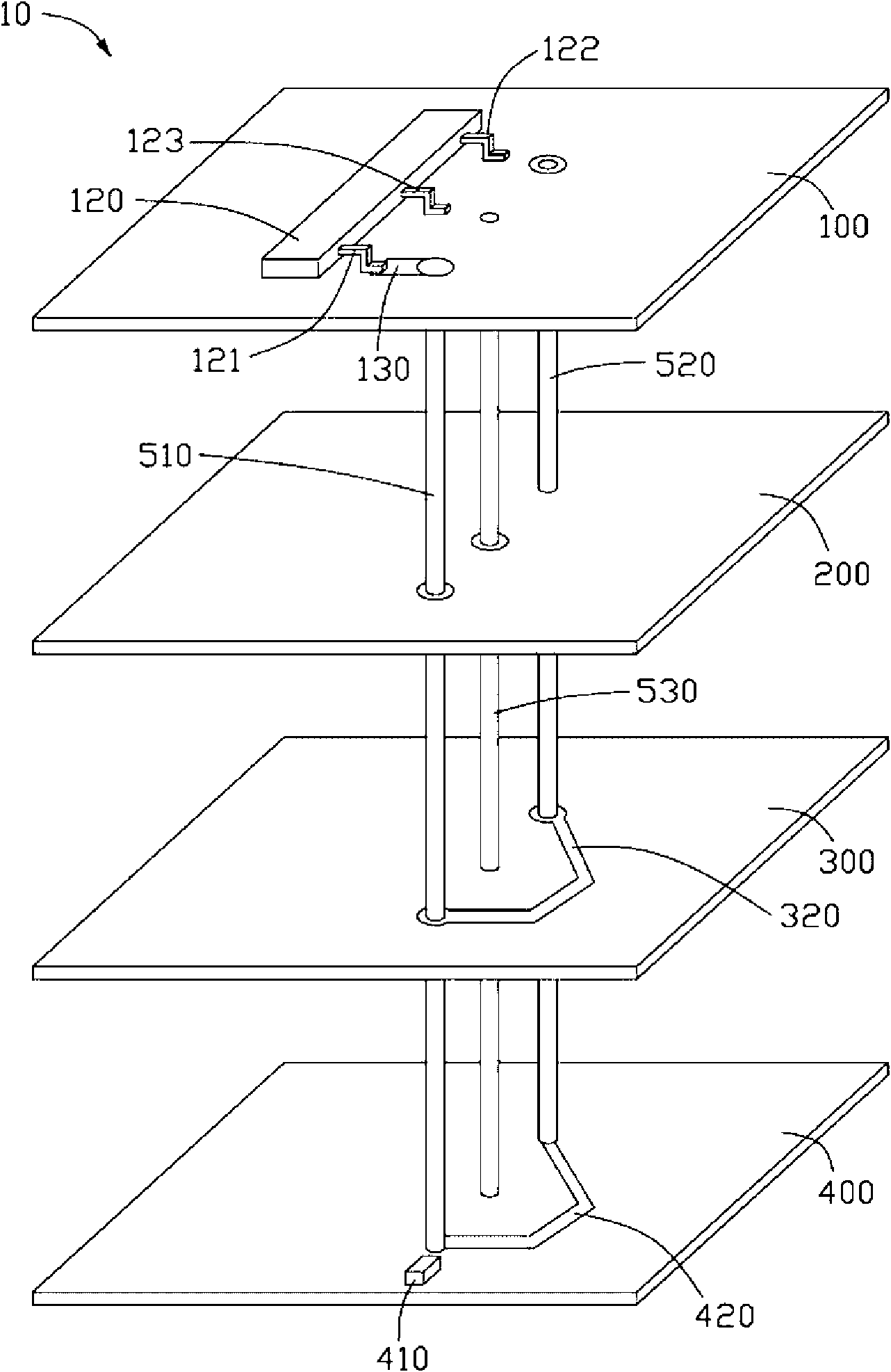
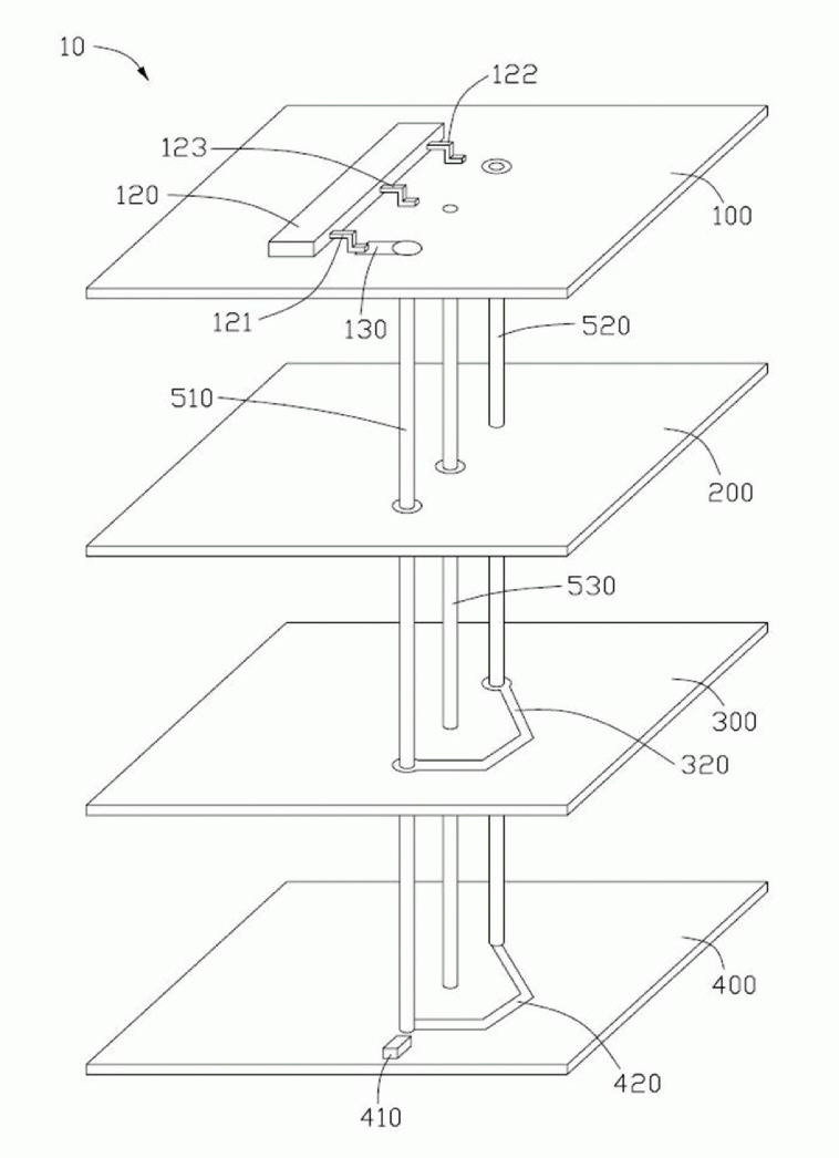
[0009] Please refer to figure 1 A preferred embodiment of the printed circuit board 10 of the present invention includes a first signal layer 100, a first reference layer (such as a power layer 200), a second reference layer (such as a ground layer 300), a second signal layer 400 . A first power supply via hole 510 , a second power supply via hole 520 and a ground via hole 530 . The power supply layer 200 is located below the first signal layer 100 , which is a power supply system of the printed circuit board 10 and is used for supplying power to components on the printed circuit board 10 . The ground layer 300 is located below the power layer 200 and above the second signal layer 400 . The first power via 510 , the second power via 520 and the ground via 530 are through holes penetrating the first signal layer 100 , the power layer 200 , the ground layer 300 and the second signal layer 400 . In this embodiment, between the first signal layer 100 and the power layer 200 , be...
PUM
 Abstract
Description
Claims
Application Information