Semiconductor device, and method for manufacturing the same

A manufacturing method and semiconductor technology, applied in semiconductor/solid-state device manufacturing, semiconductor devices, electric solid-state devices, etc., can solve problems such as difficulty in forming high-performance transistors and reduced carrier mobility

Active Publication Date: 2012-09-19
UNISANTIS ELECTRONICS SINGAPORE PTE LTD
View PDF2 Cites 0 Cited by
  • Summary
  • Abstract
  • Description
  • Claims
  • Application Information

AI Technical Summary

Problems solved by technology

Therefore, unevenness is transferred to the surface of the channel portion formed on the sidewall of the contact hole, reducing the mobility of carriers, making it difficult to form a high-performance transistor.
In addition, the contact hole size of the 65nm generation LSI manufactured now is about 80nm. If the contact hole will become more finer in the future, it is necessary to use sufficient yield to convert epitaxial silicon from such a fine contact hole. It is difficult to form a film on the bottom

Method used


Image

  • Semiconductor device, and method for manufacturing the same
  • Semiconductor device, and method for manufacturing the same
  • Semiconductor device, and method for manufacturing the same

Examples


Embodiment 1

[0381] figure 1 is an equivalent circuit using the CMOS inverter of the present invention. Hereinafter, the circuit operation of the CMOS inverter will be described. The input signal Vin1 is applied to the gates of both Qn11 belonging to NMOS and Qp11 and Qp12 belonging to PMOS. When Vin1 is "1", Qn11 belonging to NMOS will be in ON state, Qp11 and Qp12 belonging to PMOS will be in OFF state, and Vout1 will be in "0". On the contrary, when Vin1 is "0", Qn11 belonging to NMOS will be OFF, Qp11 and Qp12 belonging to PMOS will be ON, and Vout1 will be "1". As described above, the CMOS inverter operates so that the signal of Vout1 which is the output value becomes an inverse value with respect to the signal of Vin1 which is the input value.

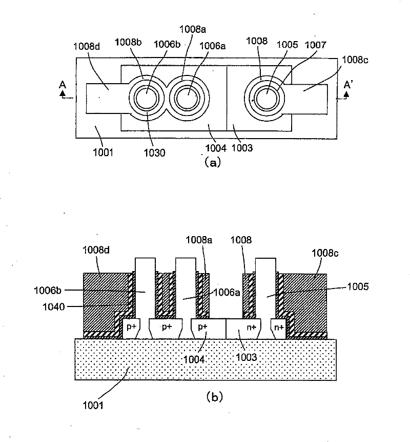
[0382] figure 2 is a plan view of a CMOS inverter using the present invention. image 3 (a) and (b) are figure 2 Sectional view of tangent line A-A' and B-B' in . Below, refer to figure 2 and image 3 To illustrate the present in...

Embodiment 2

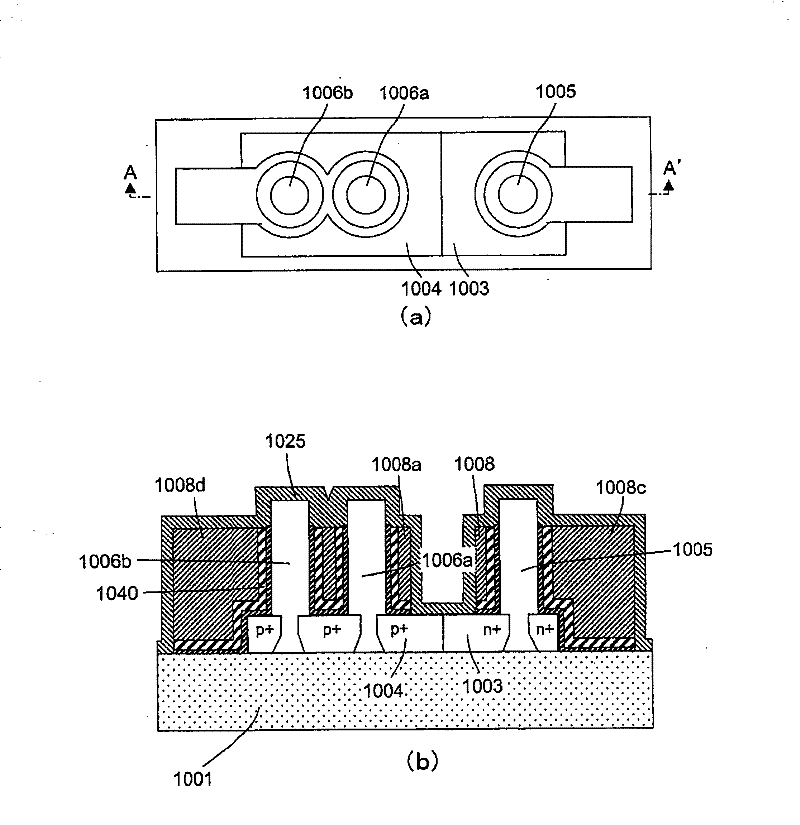
[0430] The present embodiment is an embodiment in which a CMOS inverter is configured by SGT having a structure in which a silicide layer is formed on the drain diffusion layer formed on the entire surface of the planar silicon layer and the source diffusion layer on the columnar silicon layer. By forming the silicide layer on the entire surface of the drain diffusion layer formed on the planar silicon layer, the parasitic resistance of the drain diffusion layer can be reduced. In addition, by forming a silicide layer on the source diffusion layer on the columnar silicon layer, the parasitic resistance of the source diffusion layer can be reduced. The silicide layer formed on the drain diffusion layer and the source diffusion layer can be formed only on the drain diffusion layer and the source diffusion layer in the same step in a self-aligned manner.

[0431] Figure 32 is an equivalent circuit using the CMOS inverter of the present invention. Hereinafter, the circuit opera...

Embodiment 3

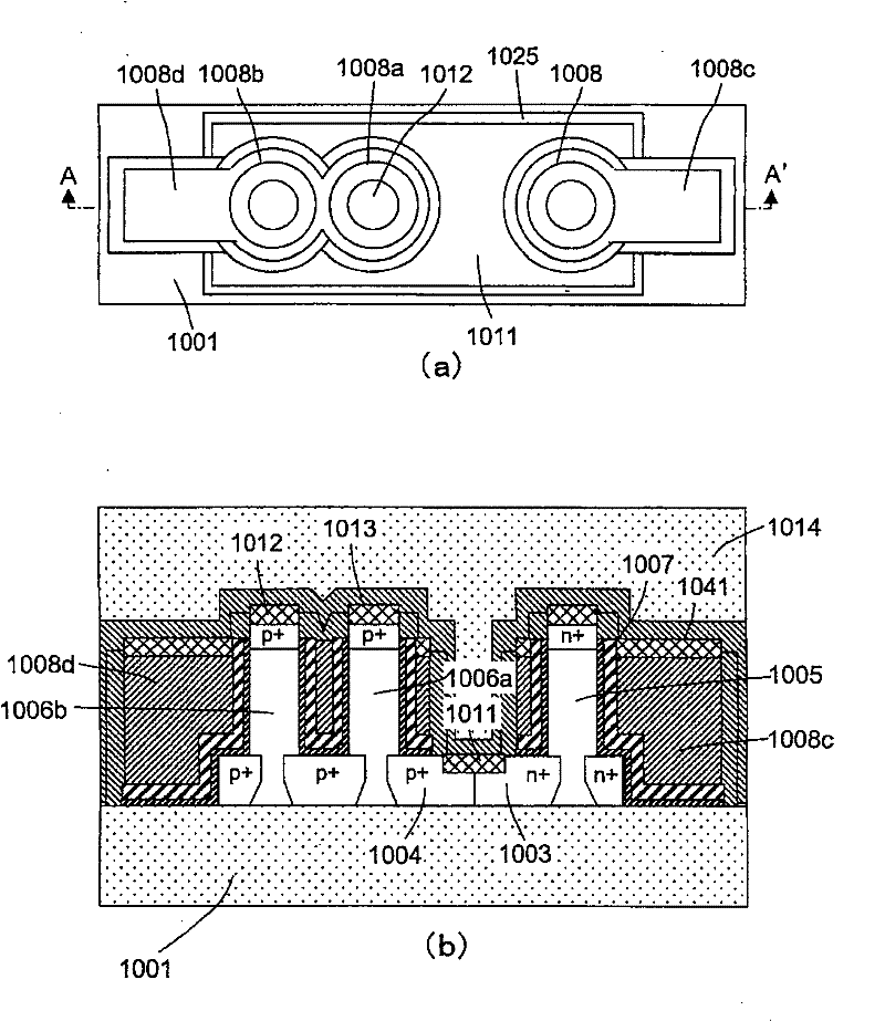
[0452] The present example is an example of an SGT having a structure in which a contact portion formed on an upper portion of a columnar silicon layer is shared by a plurality of columnar silicon layers.

[0453] Figure 43 is an equivalent circuit using the CMOS inverter of the present invention. Since the circuit operation of the CMOS inverter is the same as that of Embodiment 2, it is omitted here.

[0454] Figure 44 is a plan view of a CMOS inverter using the present invention. Figure 45 (a) and (b) are Figure 44 Sectional view of tangent line A-A' and B-B' in .

[0455] The difference between this embodiment and Embodiment 2 is that in this example, the source diffusion layer on the upper part of the two adjacent columnar silicon layers (306a, 306b) of Qp41, Qp42 belonging to PMOS is formed by sharing The rectangular contact portion 316c is connected. Specifically, when the interval between adjacent columnar silicon layers is smaller than the minimum contact por...


PUM


Abstract

Provided is a semiconductor device having a circuit, in which either a drain or source of a first MOS transistor and either a drain or source of a second MOS transistor are connected. The semiconductor device comprises a substrate, an insulating film over the substrate, and a planar semiconductor layer formed over the insulating film over the substrate. The first MOS transistor includes a first drain / source region formed in the planar semiconductor layer, a columnar semiconductor layer formed over the planar semiconductor layer, a second source / drain region formed in the upper portion of the planar semiconductor layer, and a gate formed inthe side wall of the columnar semiconductor layer. The second MOS transistor includes a third drain / source region formed in the planar semiconductor layer, a columnar semiconductor layer formed over the planar semiconductor layer, a fourth source / drain region formed in the upper portion of the columnar semiconductor layer, and a gate formed in the side wall of the columnar semiconductor layer. The semiconductor device is characterized in that a silicide layer is formed to connect at least a portion of the upper portion of the first drain / source region and at least a portion of the upper portion of the third drain / source region.

Description

technical field [0001] The present invention relates to a kind of semiconductor device and its manufacturing method, especially a kind of SGT ( Surrounding Gate Transistor (Surrounding Gate Transistor) structure and manufacturing method. Background technique [0002] In order to achieve high integration and high performance of semiconductor devices, there has been proposed a vertical transistor SGT in which a columnar semiconductor is formed on the surface of a semiconductor substrate and a gate is formed on the sidewall of the columnar semiconductor (for example, , refer to Patent Document 1 and Patent Document 2). The source, the gate, and the drain of the SGT are arranged vertically, so compared with the planar transistor in the prior art, the occupied area can be greatly reduced. In addition, since the gate surrounds the channel region, the controllability of the channel by the gate can be effectively improved as the size of the columnar semiconductor is reduced, and a...

Claims


Application Information

Patent Timeline
Patent Type & Authority Patents(China)
IPC IPC(8): H01L29/786H01L21/28H01L21/336H01L21/8238H01L27/08H01L27/092H01L29/78
CPCH01L21/823814H01L27/092H01L29/66666H01L21/823885H01L21/84H01L27/12H01L21/823821H01L29/78642H01L27/1203
Inventor 舛冈富士雄新井绅太郎
Owner UNISANTIS ELECTRONICS SINGAPORE PTE LTD
Why Eureka
Try Eureka