FPGA-based SFI4.1 device
A technology of SFI4.1 and ASIC chips, which is applied in the field of OTN, can solve the problems affecting the correct reception and transmission of data, and the difficulty of implementing 10G signal interface, so as to achieve the effect of enhancing flexibility
- Summary
- Abstract
- Description
- Claims
- Application Information
AI Technical Summary
Problems solved by technology
Method used
Image
Examples
Embodiment Construction
[0034] The present invention will be described in further detail below in conjunction with the accompanying drawings.
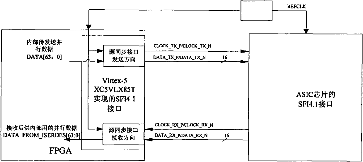
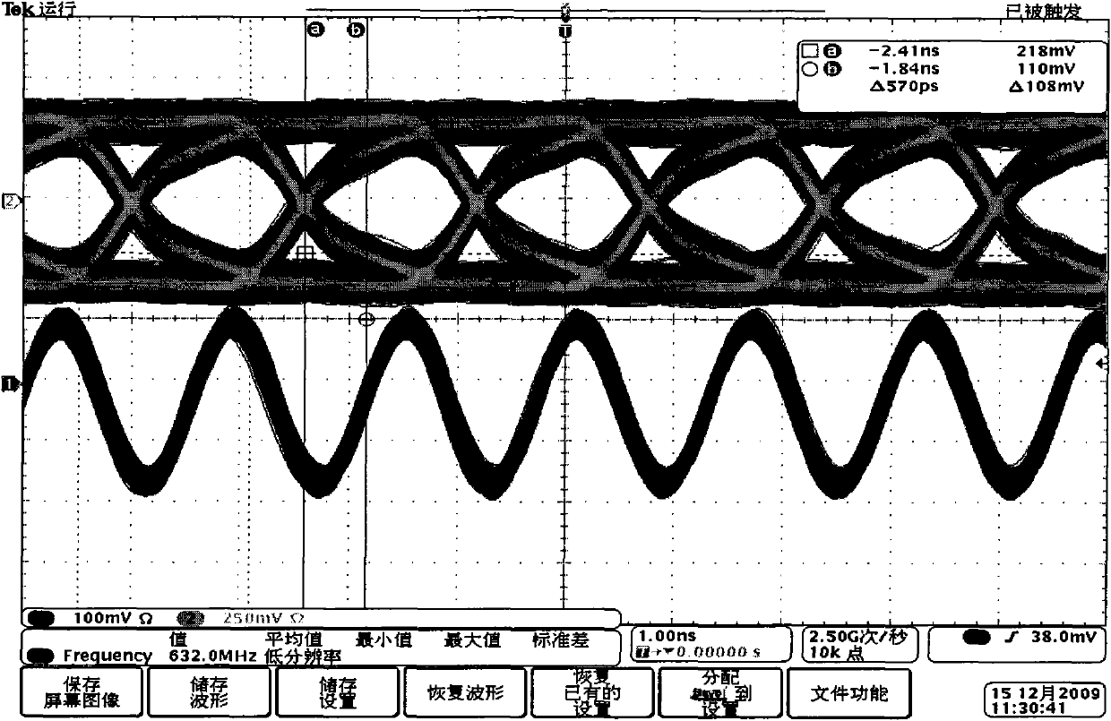
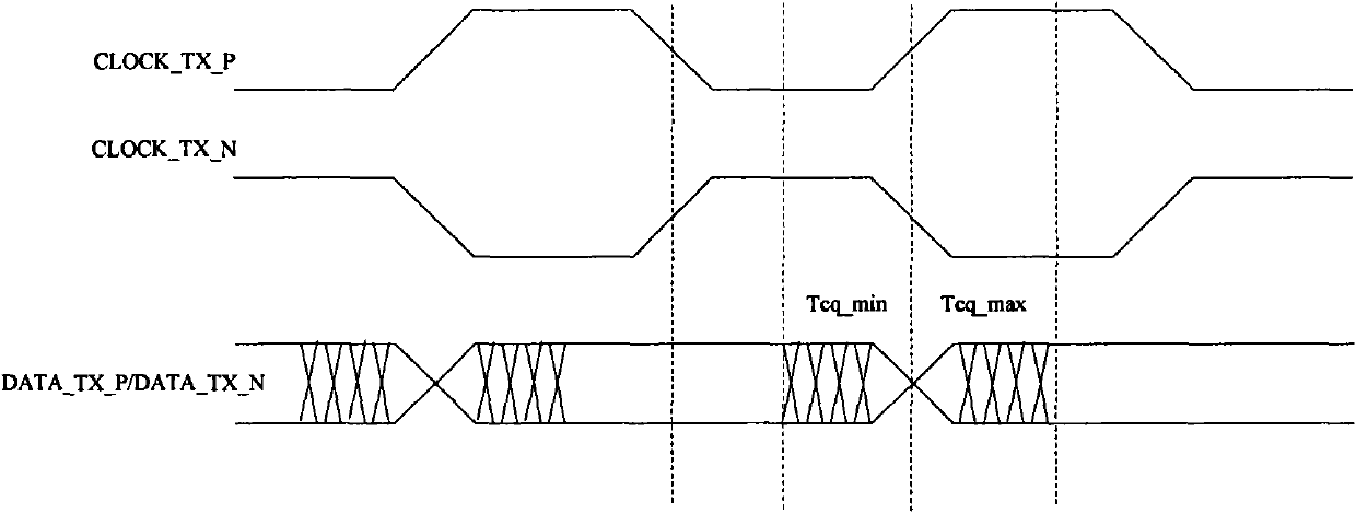
[0035]The present invention is applied in the OTN system equipment, and part of the line cards in the OTN system equipment internally process the ODU2 signal transmitted by the SFI4.1 interface. The present invention realizes the SF4.1 interface in the FPGA and completes the transmission by the SFI4.1 interface. The ODU2 signal is correctly received in the FPGA and sent after processing. The SFI4.1 interface uses 16 pairs of differential data lines and a pair of differential clocks to simultaneously transmit data signals, which is a high-speed source synchronous interface. The single-channel data rate of the SFI4.1 interface in the actual OTN system equipment is 627.33Mb / s. At the receiving end, the input high-speed parallel source synchronous signal satisfies the SFI4.1 interface clock-data relationship proposed by OIF. Since the internal clock signal and d...
PUM
 Abstract
Description
Claims
Application Information


