Optical element
An optical element, visible light technology, applied in optical elements, optics, instruments, etc., can solve problems such as low-reflection structures, and achieve high anti-reflection properties, excellent anti-reflection properties, and high productivity.
- Summary
- Abstract
- Description
- Claims
- Application Information
AI Technical Summary
Problems solved by technology
Method used
Image

Examples
no. 1 approach
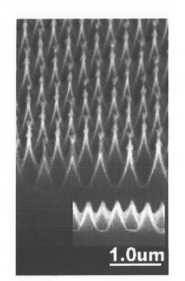
[0072] (1-1) Structure of optical element
[0073] Figure 8A is a schematic plan view showing a structural example of the optical element according to the first embodiment of the present invention. Figure 8B yes Figure 8A An enlarged plan view of a portion of the optical components shown. Figure 8C is along Figure 8B Sectional views taken of tracks T1, T3, . . . are shown. Figure 8D is along Figure 8B Sectional views of the tracks T2, T4, . . . shown.
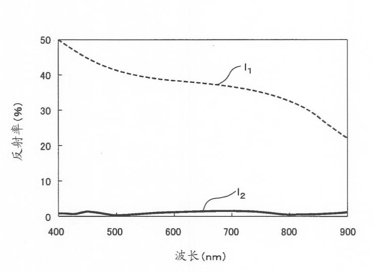
[0074] The optical element 1 is applicable to various optical devices such as displays, optoelectronic devices, optical communication devices (optical fibers), solar cells, and lighting devices. For example, the optical element 1 can be used for an antireflection substrate and a light guide plate suitable for preventing reflection of light having a wavelength range of visible light. Furthermore, the optical element 1 can be used for an optical filter having transmittance according to an incident angle of incident ...
no. 2 approach
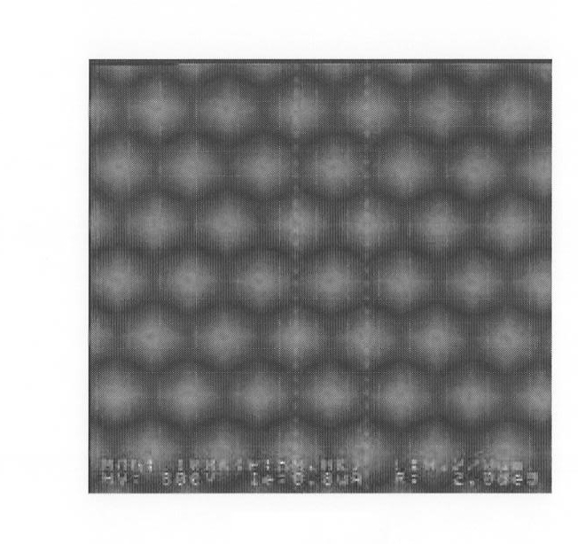
[0136] (2-1) Structure of optical element
[0137] Figure 15A is a schematic plan view showing a structural example of an optical element according to a second embodiment of the present invention. Figure 15B yes Figure 15A An enlarged plan view of a portion of the optical components shown. Figure 15C is along Figure 15B Sectional views taken of tracks T1, T3, . . . are shown. Figure 15D is along Figure 15B Sectional views of the tracks T2, T4, . . . shown.
[0138] In the optical element 1 according to the second embodiment, the track T has an arc shape, and the main structures 3 are arranged in the arc shape. Such as Figure 15B As shown, in the tracks (T1~T3) of three adjacent rows, the main structures 3 are arranged to form a quasi-hexagonal lattice pattern having the centers of the main structures 3 positioned at points a1~a7. The term "quasi-hexagonal lattice pattern" refers to a hexagonal lattice pattern in which the arc shape along a track T is distorted ...
no. 3 approach
[0153] Figure 18A is a schematic plan view showing a structural example of an optical element according to a third embodiment of the present invention. Figure 18B yes Figure 18A An enlarged plan view of a portion of the optical components shown. Figure 18C is along Figure 18B Sectional views taken of tracks T1, T3, . . . are shown. Figure 18D is along Figure 18B Sectional views of the tracks T2, T4, . . . shown.
[0154] The optical element 1 according to the third embodiment differs from the first embodiment in that in the tracks of three adjacent rows the primary structures 3 form a tetragonal lattice pattern or a quasi-tetragonal lattice pattern. The term "quasi-tetragonal lattice pattern" refers to a tetragonal lattice pattern that is stretched and distorted in the direction of track extension (X direction) different from a regular tetragonal lattice pattern. When the main structures 3 are periodically arranged in a tetragonal lattice pattern or a quasi-tetrag...
PUM
| Property | Measurement | Unit |
|---|---|---|
| diameter | aaaaa | aaaaa |
| diameter | aaaaa | aaaaa |
| depth | aaaaa | aaaaa |
Abstract
Description
Claims
Application Information