Electronic component inspecting method and apparatus used in the method

A technology for electronic components and inspection methods, applied in measurement devices, instruments, material analysis by optical means, etc., can solve the problems of high-speed limitation, difficulty in accurately measuring distance, and time-consuming adjustment, and achieve high-speed operation. , to achieve the effect of miniaturization and shortening of time

Inactive Publication Date: 2011-01-26
KYODO DESIGN & PLANNING CORP
View PDF2 Cites 24 Cited by
  • Summary
  • Abstract
  • Description
  • Claims
  • Application Information

AI Technical Summary

Problems solved by technology

However, the conventional autofocus function uses reflected light from the subject to measure the distance to calculate the focal length. Therefore, it is difficult to accurately measure the distance from the microscope to the uneven surface of fine electronic components, and the distance from the back side of the transparent substrate to the distance that can be seen through the transparent substrate. Questions like the distance to the indentation
Therefore, recently, an autofocus function using a special laser-type displ

Method used


Image

  • Electronic component inspecting method and apparatus used in the method
  • Electronic component inspecting method and apparatus used in the method
  • Electronic component inspecting method and apparatus used in the method

Examples


Embodiment Construction

[0044] Next, the best mode for carrying out the present invention will be described.

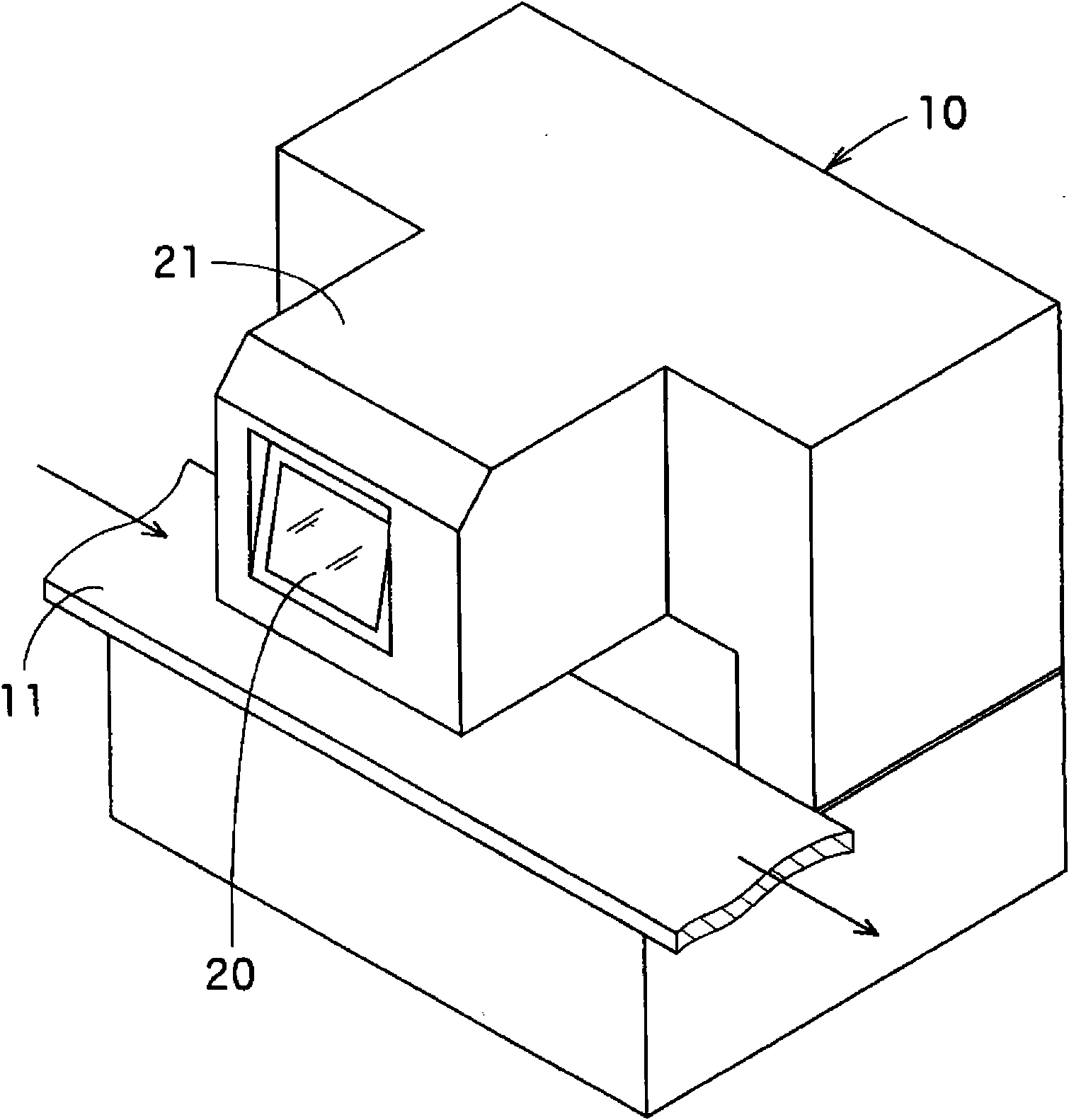
[0045] figure 1 It is an external perspective view showing one embodiment of the electronic component inspection apparatus of the present invention. This inspection device 10 is arranged on the side of the conveyer belt 11 that is connected with the LCD assembly production line, and the manufactured LCD assemblies are taken in from the conveyer belt 11 to the stage in the inspection device 10 for inspection, and then the inspected The last LCD assembly returns to the conveyor belt 11. In addition, reference numeral 20 is a monitor screen for displaying images obtained during the above inspection, and reference numeral 21 is a main body including a control management unit for controlling the operation of the device and an information processing unit for inspection.

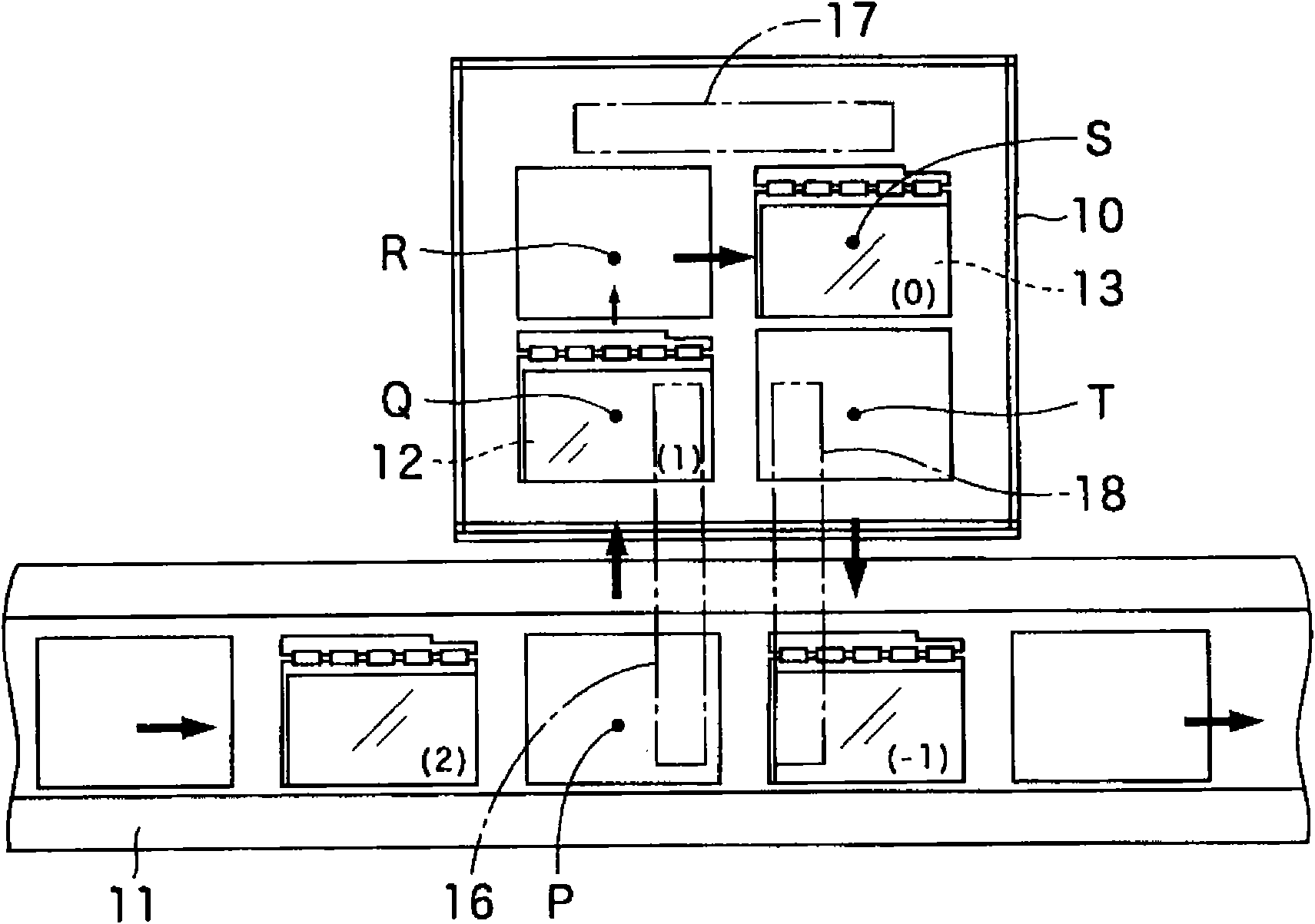
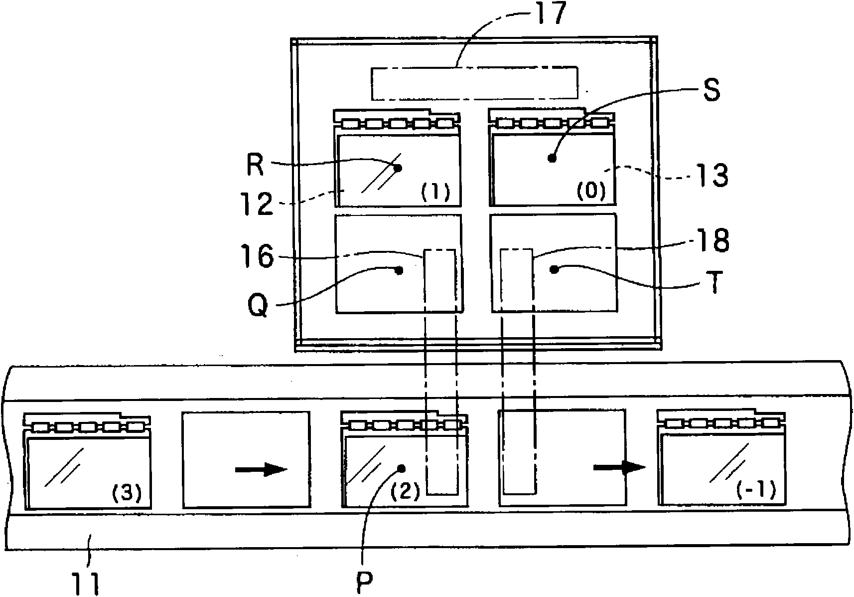
[0046] And, if Figure 2A As shown, in this inspection device, two stages 12 and 13 for inspection are arranged in parallel...


PUM


Abstract

Provided is an excellent inspecting method for quickly and correctly inspecting fine sections of an electronic component. An apparatus used in such method is also provided. An electronic component is placed on a stage, and an imaging means (40) provided by combining a differential interference microscope (44) and a CCD camera (45) is aligned by being moved by an X-direction moving means (46). As for an electronic component to be inspected first, an objective lens of the differential interference microscope (44) is advanced/retracted by means of a Z-direction adjusting means (47), and a plurality of images are continuously picked up. Then, an optimum focal point distance is calculated from the image data to perform focusing, then, an image is picked up. As for the subsequent electronic components, an image is picked up after performing automatic focusing, corresponding to a predicted optimum focal point distance derived from the optimum foal point distance stored in previous inspection or before, and whether the imaged portion is acceptable or not is inspected, based on the obtained image data.

Description

technical field [0001] The present invention relates to a method for inspecting microscopic defects and presence or absence of foreign matter of various electronic components and an apparatus used in the method. Background technique [0002] In recent years, in electronic components such as liquid crystal displays (LCDs), optical devices, and semiconductor devices, there has been a rapid development in the sophistication and refinement of mounting technology along with the increase in processing capacity and high integration. Therefore, on the production line of such high-density mounted electronic components, it is becoming more and more important to quickly and accurately inspect whether patterning of circuits, connections between members are appropriate, or whether foreign matter is mixed. [0003] For example, an LCD module can be obtained by mounting a driving chip on the edge of a glass substrate of a liquid crystal panel in a COG manner, and connecting the driving chi...

Claims


Application Information

Patent Timeline
IPC IPC(8): G01N21/88G01N21/85
CPCG01N21/95684
Inventor 津田仁彦张春生后藤哲郭卫红
Owner KYODO DESIGN & PLANNING CORP
Why Eureka
Try Eureka