Organic electro-luminescence display unit and manufacturing thereof

A technology of electroluminescence and display unit, which is applied in the direction of electrical components, semiconductor/solid-state device manufacturing, circuits, etc. It can solve the problems of inability to display brightness, affect the accuracy of light sensors, and effectively reduce the power consumption of organic electroluminescence displays, etc. question

Active Publication Date: 2011-02-02
AU OPTRONICS CORP
View PDF7 Cites 20 Cited by
  • Summary
  • Abstract
  • Description
  • Claims
  • Application Information

AI Technical Summary

Problems solved by technology

However, the disadvantage of this prior art is that the single light sensor is easily disturbed by the scanning circuit, ambient temperature or other factors, thus affecting the accuracy of the light sensor.
In the case where the light sensor cannot effectively adjust the brightn

Method used


Image

  • Organic electro-luminescence display unit and manufacturing thereof
  • Organic electro-luminescence display unit and manufacturing thereof
  • Organic electro-luminescence display unit and manufacturing thereof

Examples


no. 1 example

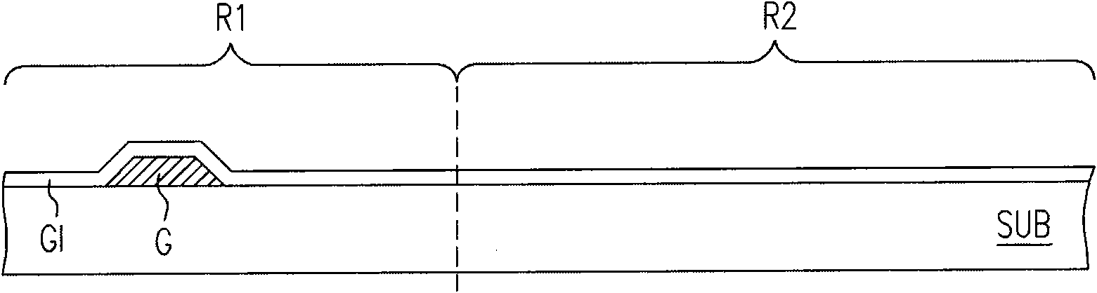
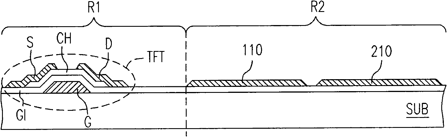
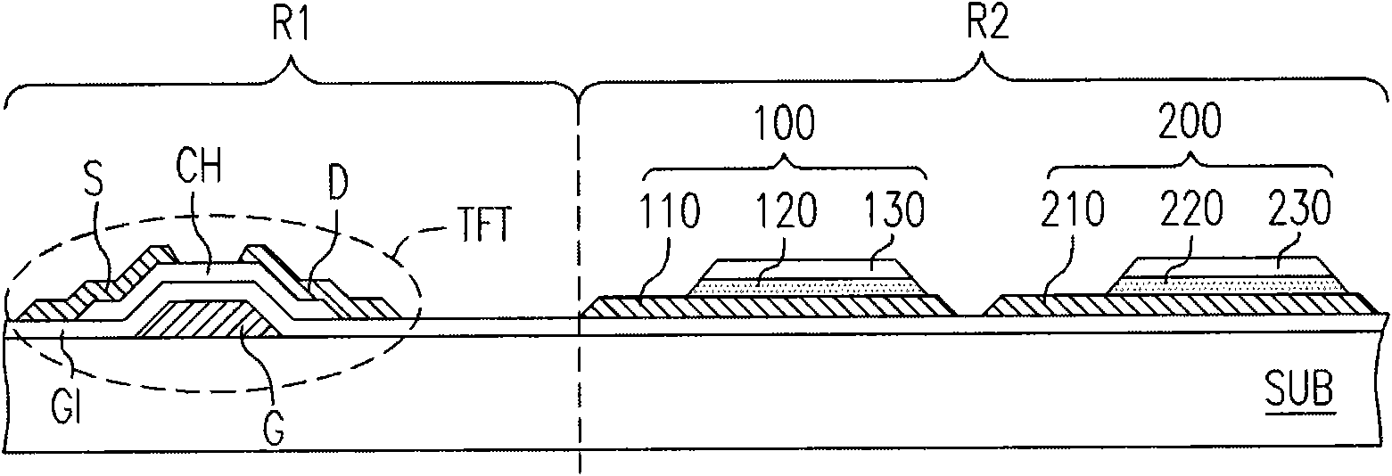
[0060] Figure 1A to Figure 1E It is a schematic cross-sectional view of the manufacturing process of the organic electroluminescent display unit according to the first embodiment of the present invention. First, please refer to Figure 1A , providing a substrate SUB, the substrate SUB has a display region R1 and a peripheral region R2. Then at least one gate G is formed on the substrate SUB ( Figure 1A Only one gate is shown in the figure), and a gate insulating layer GI is formed on the substrate SUB to cover the gate G. In other words, the gate insulating layer GI covers the display region R1 and the peripheral region R2 mentioned above. In this embodiment, the material of the substrate SUB is, for example, glass, quartz, organic polymer, opaque / reflective material (such as conductive material, wafer, ceramic, or other applicable material), or other applicable Material. In addition, the above-mentioned display region R1 is a region for forming organic electroluminescen...

no. 2 example

[0077] Figure 2A to Figure 2E It is a schematic cross-sectional view of the manufacturing process of the organic electroluminescence display unit according to the second embodiment of the present invention. The manufacturing process of the organic electroluminescence display unit of this embodiment is similar to that of the first embodiment, but the main difference between them is that the connection mode between the first light sensor 100 and the second light sensor 200 is different. Such as Figure 2D As shown, the first transparent top electrode 130 is only electrically connected to the leftmost bridge pattern 330, the second reflective bottom electrode 210 is only electrically connected to the rightmost bridge pattern 330, and the first reflective bottom electrode 110 is electrically connected to the second The two transparent top electrodes 230 are electrically connected to each other through the middle bridge pattern 330 and the light-shielding pattern 320 .

[0078] ...


PUM


Abstract

The invention relates to an organic electro-luminescence display unit, which comprises at least one transistor, a first photo sensor, a second photo sensor, a reflective conducting layer, an organic electro-luminescence layer and a cathode layer, wherein the transistor is electrically connected with a scanning line and a data line; the first photo sensor comprises a first reflective bottom electrode, a first photosensitive layer and a first transparent top electrode; the second photo sensor comprises a second reflective bottom electrode, a second photosensitive layer and a second transparent top electrode; the first photo sensor is electrically connected with the second photo sensor; the reflective conducting layer comprises a pixel electrode, a shading pattern and a bridging pattern; the pixel electrode is electrically connected with the transistor; the shading pattern is electrically connected with the second transparent top electrode and completely covers the second photosensitive layer; and the bridging pattern is electrically connected with the first transparent top electrode, the first reflective bottom electrode and the second reflective bottom electrode.

Description

technical field [0001] The present invention relates to a display unit and its manufacturing method, and in particular to an organic electroluminescent display unit and its manufacturing method. Background technique [0002] Recently, the awareness of environmental protection has risen, and flat display panels (flat display panels) with superior characteristics such as low power consumption, good space utilization efficiency, no radiation, and high image quality have become the mainstream of the market. Common flat panel displays include liquid crystal displays, plasma displays, organic electroluminescent displays, and the like. Taking the organic electroluminescent display as an example, it is a self-luminous display without a backlight module, so the manufacturing cost of the backlight module and the energy consumed by the backlight module itself can be saved. In addition, since the organic electroluminescent display has no viewing angle problem, and has the characteristi...

Claims


Application Information

Patent Timeline
IPC IPC(8): H01L21/77H01L27/32
Inventor 常鼎国方俊雄
Owner AU OPTRONICS CORP
Why Eureka
Try Eureka