

Pulse width signal duty ratio detection circuit
A technology of duty ratio detection and pulse width signal, which is applied in the direction of monitoring pulse chain mode, etc., can solve the problems of long time, large area, and reduction of integrated circuit integration, and achieve the effect of improving reliability and integration
- Summary
- Abstract
- Description
- Claims
- Application Information
AI Technical Summary
Problems solved by technology
Method used
Image

Examples
Embodiment 1
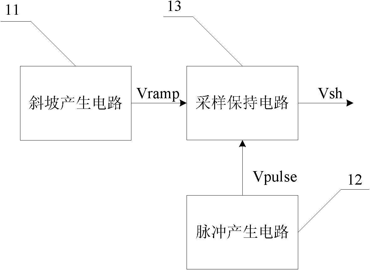
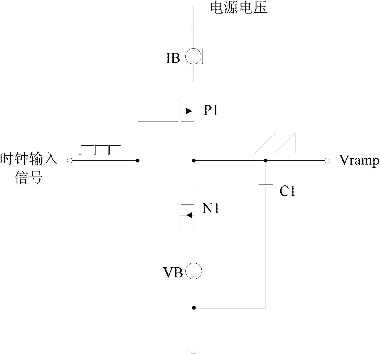
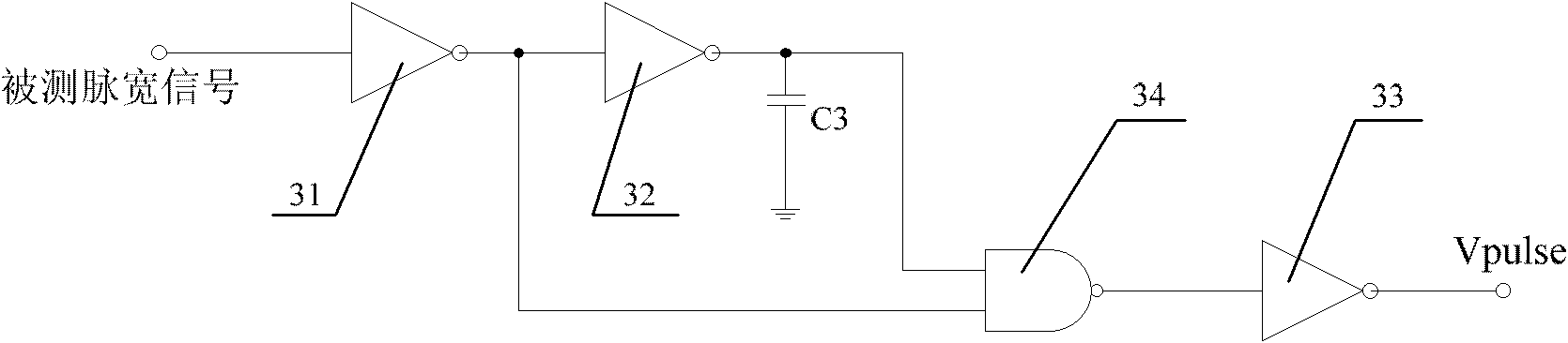
[0024] A pulse width signal duty cycle detection circuit proposed by the present invention, its block diagram is as follows figure 1 As shown, it includes a ramp generating circuit 11, a pulse generating circuit 12 and a sample-and-hold circuit 13. The input terminal of the ramp generating circuit 11 inputs a clock input signal, and the ramp generating circuit 11 outputs a fixed ramp signal Vramp according to the clock input signal (such as Figure 6c shown), the cycle of the ramp signal Vramp is related to the measured pulse width signal (such as Figure 6a shown) have the same cycle size, and the voltage value of the ramp signal Vramp changes from the voltage value V1 to the voltage value V2 within one cycle, such as Figure 6c Shown; The pulse generation circuit 12 is used for monitoring the falling edge of the measured pulse width signal, and the input terminal input of the pulse generation circuit 12 is as Figure 6a As shown in the measured pulse width signal, the puls...
Embodiment 2
[0035] The circuit structure of this embodiment is basically the same as that of Embodiment 1, the only difference is that the sample and hold circuit 13 is connected with a voltage buffer amplifier circuit 14, such as Figure 5 As shown, the voltage buffer amplifier circuit 14 is used to buffer the voltage value Vsh output by the output terminal of the sample and hold circuit 13, so as to improve the driving capability of the circuit. The input terminal of the voltage buffer amplifier circuit 14 inputs the voltage value output by the sampling and holding circuit 13, the voltage buffer amplifier circuit 14 amplifies the input voltage value, and the output terminal of the voltage buffer amplifier circuit 14 outputs the amplified voltage value Vo, as Figure 6e As shown, the amplified voltage value Vo is equal to the product of the gain A of the voltage buffer amplifier circuit 14 and the voltage value Vsh output by the sample-and-hold circuit 13, that is, Vo=A×Vsh=A×[ V1+(V2-V1)...
PUM
 Abstract
Description
Claims
Application Information