Process of antireflection coating battery capable of reducing surface recombination
A technology of surface compounding and anti-reflection film, which is applied in the direction of circuits, electrical components, sustainable manufacturing/processing, etc., can solve the problem of battery performance degradation, achieve the effect of reducing process and improving battery efficiency
- Summary
- Abstract
- Description
- Claims
- Application Information
AI Technical Summary
Problems solved by technology
Method used
Image
Examples
Embodiment 1
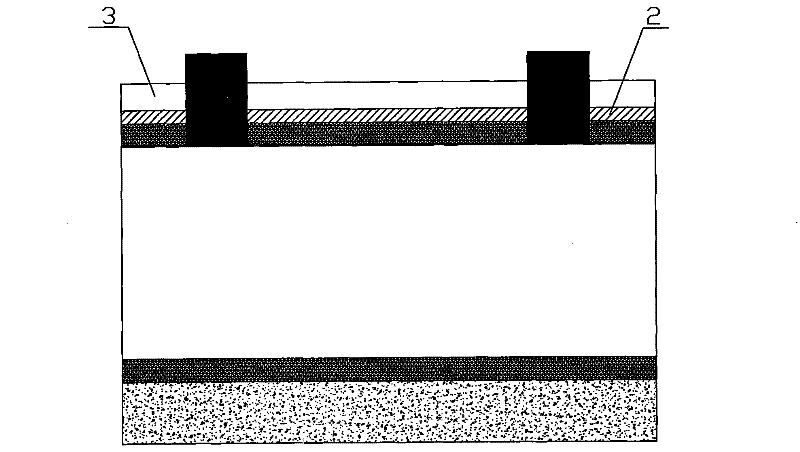
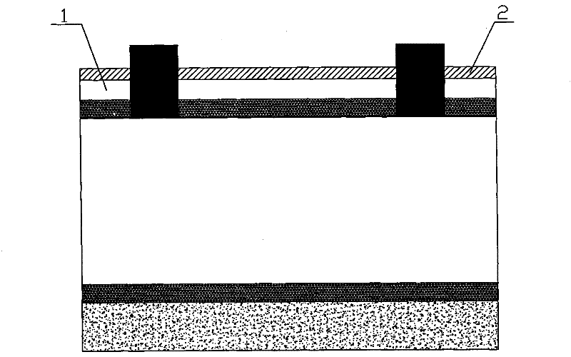
[0013] Such as figure 2 Shown is a schematic diagram of the structure of Embodiment 1 of the present invention, the process of reducing the surface composite anti-reflection film battery has the following process steps: a. Diffusion treatment is performed on the silicon wafer; b. Then PSG and edge cutting are performed on the silicon wafer; c . Then carry out anti-reflection and passivation film treatment on the surface of the silicon wafer; d. Then perform RIE texturing on the surface of the silicon wafer after anti-reflection and / or passivation treatment; e. Finally, perform screen printing and sinter to make a finished product.
[0014] The anti-reflection passivation film in the above-mentioned embodiment 1 adopts S i N film with a thickness of 1um; after the anti-reflection film process is completed, the RIE texturing process is carried out directly on the S i The RIE texture layer 2 is formed on the N surface.
[0015] Under this technological process, the reflectance...
Embodiment 2
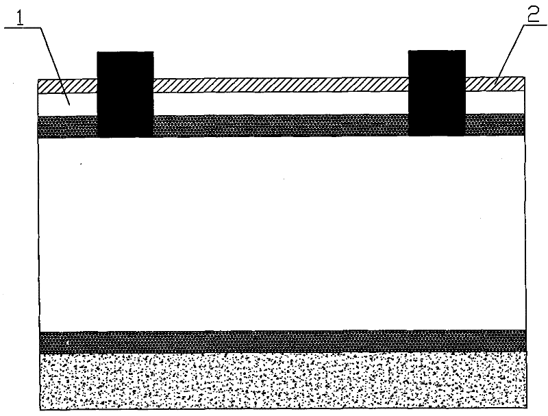
[0017] The process of reducing the surface composite anti-reflection film battery has the following process steps: a. Diffusion treatment on the silicon wafer; b. Then PSG removal and edge cutting treatment on the silicon wafer; c. Passivation film treatment on the surface of the silicon wafer; d. Carry out RIE texturing on the surface of the silicon wafer after passivation treatment; e. Carry out anti-reflection film treatment on the surface of the silicon wafer after texturing; f. Finally, carry out screen printing and sintering to make a finished product.
[0018] The passivation film in the above-mentioned embodiment two adopts S i o 2 film, the thickness is 1um; the anti-reflection film adopts S i N film with a thickness of 80nm; this process is in S i o 2 Carry out RIE texturing on the layer, and then use S i N film for covering, using S i o 2 Passivation can achieve a better surface passivation effect, plus RIE texturing and S i The surface anti-reflection treatm...
PUM
 Abstract
Description
Claims
Application Information
 - R&D
- Intellectual Property
- Life Sciences
- Materials
- Tech Scout
- Unparalleled Data Quality
- Higher Quality Content
- 60% Fewer Hallucinations
Browse by: Latest US Patents, China's latest patents, Technical Efficacy Thesaurus, Application Domain, Technology Topic, Popular Technical Reports.
© 2025 PatSnap. All rights reserved.Legal|Privacy policy|Modern Slavery Act Transparency Statement|Sitemap|About US| Contact US: help@patsnap.com


