TFT-LCD array substrate and manufacturing method thereof

An array substrate and substrate technology, which is applied to the TFT-LCD array substrate and its manufacturing field, can solve the problems of high driving power consumption, long charging and discharging time, large voltage drop, etc., so as to eliminate the large voltage drop and shorten the charging and discharging time. , The effect of reducing drive power consumption

Inactive Publication Date: 2011-03-30
BOE TECH GRP CO LTD +1
View PDF0 Cites 15 Cited by
  • Summary
  • Abstract
  • Description
  • Claims
  • Application Information

AI Technical Summary

Problems solved by technology

Since the voltage polarities of two adjacent frames of the same pixel electrode are exactly opposite, there is a large voltage drop. Therefore, the existing polarity reversal method increases the difficulty of charging and discharging the pixel electrode. On the one hand, the charging and discharging time is longer, and on the other hand On the one hand, the drive power consumption is large

Method used


Image

  • TFT-LCD array substrate and manufacturing method thereof
  • TFT-LCD array substrate and manufacturing method thereof
  • TFT-LCD array substrate and manufacturing method thereof

Examples


Embodiment Construction

[0055] The technical solutions of the present invention will be described in further detail below with reference to the accompanying drawings and embodiments.

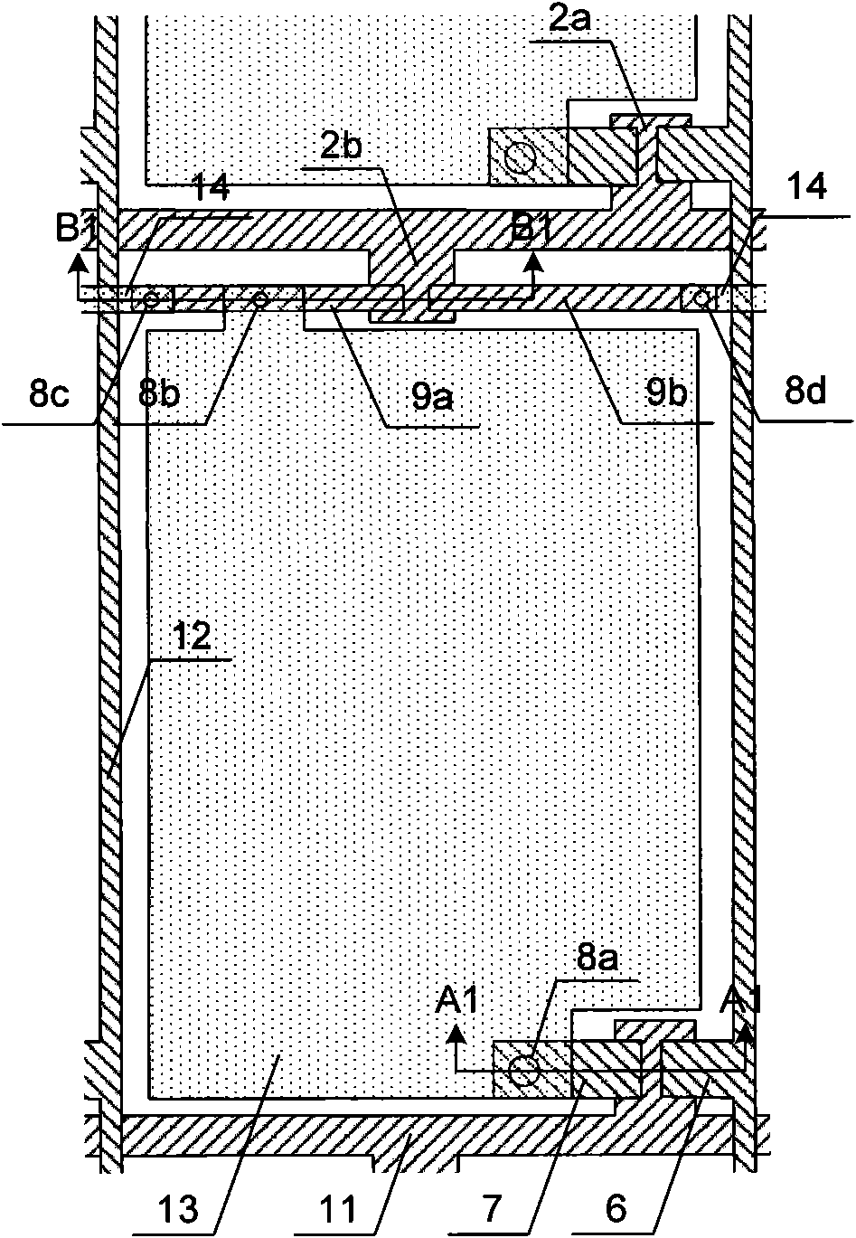
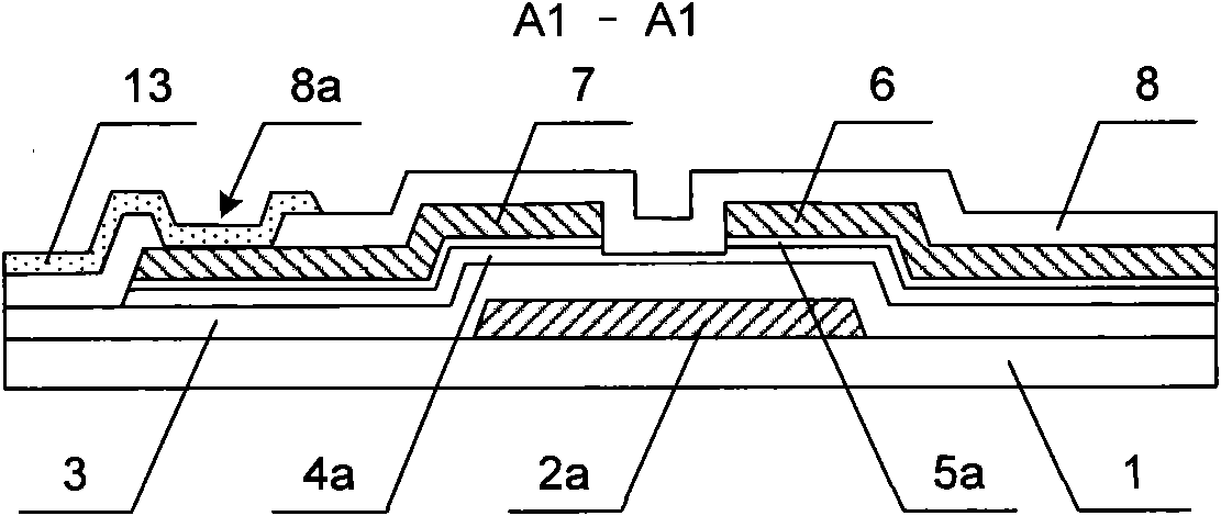
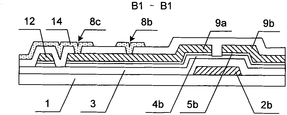
[0056] figure 1 It is a plan view of the first embodiment of the TFT-LCD array substrate of the present invention, reflecting the structure of a pixel unit, figure 2 for figure 1 The cross-sectional view of A1-A1 in the middle, image 3 for figure 1 Sectional view of B1-B1 direction in the middle. Such as Figure 1 ~ Figure 3 As shown, the main structure of the TFT-LCD array substrate in this embodiment includes gate lines 11, data lines 12, pixel electrodes 13, first thin film transistors and second thin film transistors formed on the substrate 1, several gate lines 11 and several The data lines 12 define several pixel areas arranged in a matrix, and a first thin film transistor, a second thin film transistor and a pixel electrode 13 are formed in each pixel area, wherein the first thin film transistor and the s...


PUM


Abstract

The invention relates to a TFT-LCD array substrate and a manufacturing method thereof. The array substrate comprises a gate line and a data line which are formed on a substrate and limit a plurality of pixel areas, wherein a pixel electrode, a first thin film transistor controlling charging of the pixel electrode and a second thin film transistor controlling precharging of the pixel electrode areformed in each pixel electrode. Through forming the first thin film transistor and the second thin film transistor respectively controlling charging and precharging of the pixel electrode in each pixel area, when the pixel electrodes in a pixel row are charged, the pixel electrodes in the adjacent next pixel row realize precharge, thus reducing the difference between the voltage of the frames of the pixel electrodes in the pixel row and the voltage of the next frames, effectively eliminating the defect of higher voltage drop in the polarity inversion mode, effectively shortening the charging / discharging time on the one hand and effectively reducing the drive power consumption on the other hand.

Description

technical field [0001] The invention relates to a thin film transistor liquid crystal display and a manufacturing method thereof, in particular to a TFT-LCD array substrate and a manufacturing method thereof. Background technique [0002] Thin Film Transistor Liquid Crystal Display (TFT-LCD for short) has the characteristics of small size, low power consumption, and no radiation, and occupies a dominant position in the current flat panel display market. TFT-LCD mainly includes an array substrate and a color filter substrate that are boxed together with liquid crystal interposed therebetween. Gate lines, data lines, pixel electrodes and thin-film transistors are formed on the array substrate, and each pixel electrode is controlled by a thin-film transistor. When the thin film transistor is turned on, the pixel electrode is charged during the turn-on time, and after the thin film transistor is turned off, the voltage of the pixel electrode will be maintained until recharging i...

Claims


Application Information

Patent Timeline
IPC IPC(8): G02F1/1362G02F1/1368H01L21/82
CPCG09G2300/0814H01L27/1214G09G2310/0251G09G3/3659H01L27/12G02F1/13624G09G2330/023G09G3/3614H01L27/124
Inventor 任祖兴
Owner BOE TECH GRP CO LTD
Why Eureka
Try Eureka