Method for exposing semiconductor substrate and invalidation analysis method

A semiconductor and substrate technology, which is applied in the field of failure analysis of semiconductor devices, can solve problems such as damage to semiconductor substrates, and achieve the effect of ensuring accuracy and improving accuracy

Active Publication Date: 2011-03-30
SEMICON MFG INT (SHANGHAI) CORP
View PDF1 Cites 22 Cited by
  • Summary
  • Abstract
  • Description
  • Claims
  • Application Information

AI Technical Summary

Problems solved by technology

[0006] The invention solves the problem that the semiconductor substrate will be damaged in t...

Method used


Image

  • Method for exposing semiconductor substrate and invalidation analysis method
  • Method for exposing semiconductor substrate and invalidation analysis method
  • Method for exposing semiconductor substrate and invalidation analysis method

Examples


Embodiment Construction

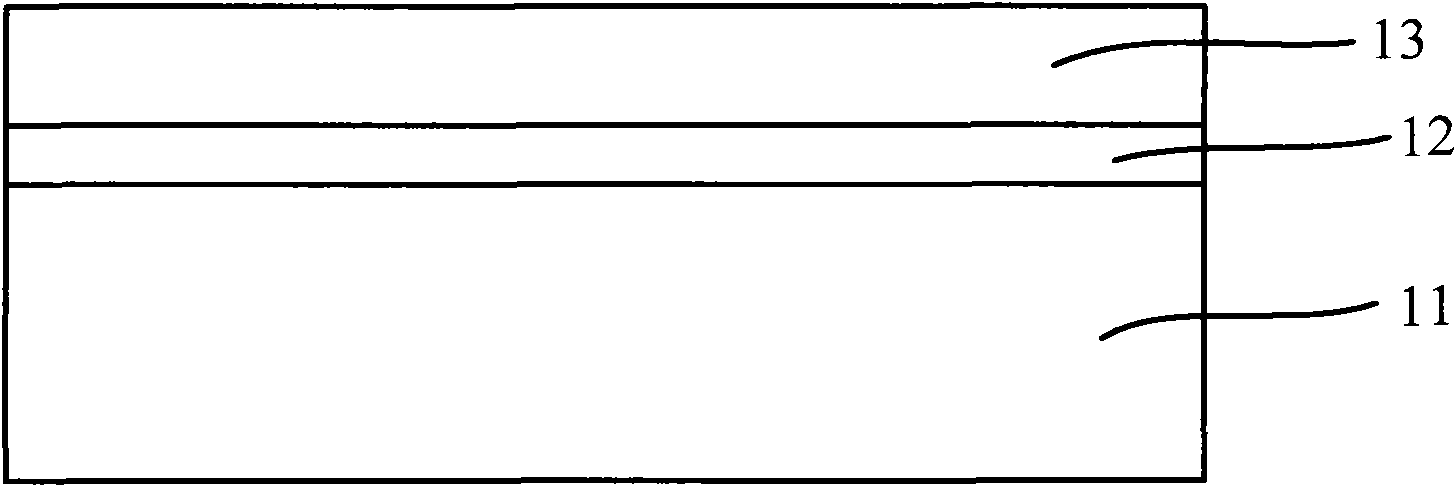
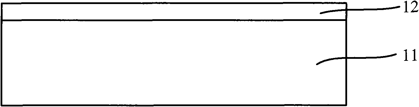
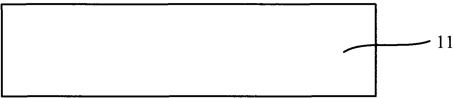
[0018] According to the analysis of the inventors, it is found that if the silicon substrate is defective, a concentrated current (or high current) will be formed in the region corresponding to the defect position between the polysilicon layer and the silicon substrate after the failure test, and the silicon dioxide layer will be broken down. When polysilicon etchant is used to remove the polysilicon layer, the polysilicon etchant will erode the silicon substrate through the concentrated current area, resulting in pits on the silicon substrate (such as Figure 4 Defect 21a) shown. In this case, if the defect analysis of the exposed silicon substrate is carried out, it is impossible to judge whether it is a defect of the substrate itself, a defect caused to the substrate during the process, or a defect caused by the substrate when the polysilicon layer is stripped. defects caused by the bottom. Therefore, peeling off the polysilicon layer and the silicon dioxide layer on the s...


PUM


Abstract

The invention provides a method for exposing a semiconductor substrate and an invalidation analysis method. The method comprises the following steps: providing a semiconductor sample; removing an oxidation layer between the semiconductor substrate and a semiconductor polycrystal layer with chemical solution; and removing the semiconductor polycrystal layer through ultrasonic oscillation and exposing the semiconductor substrate, wherein the semiconductor sample comprises the semiconductor substrate, the oxidation layer and the semiconductor polycrystal layer from bottom to top in sequence; and the chemical solution is buffer oxide etching solution or hydrofluoric acid. The method for exposing the semiconductor substrate and the invalidation analysis method solve the problem that the semiconductor substrate can be damaged by de-layering the semiconductor polycrystal layer and the oxidation layer above the semiconductor substrate by layers in the prior art.

Description

technical field [0001] The invention relates to failure analysis of semiconductor devices, in particular to a method for exposing a semiconductor substrate and a method for failure analysis of semiconductor devices. Background technique [0002] For failure analysis of semiconductor devices, it is usually to first peel off (De-layer) other layers above the target layer for defect analysis to expose the entire target layer, and then use scanning electron microscope (SEM), transmission electron A microscope (TEM) or an optical microscope (OM) etc. observes the target layer and conducts defect analysis. For example, US Pat. No. 5,935,870 discloses a failure analysis method, which uses chemical mechanical polishing (CMP), etching, etc. to peel off other layers on the gate oxide layer layer by layer, so as to expose the entire gate oxide layer. [0003] For semiconductor device failures caused by defects of the semiconductor substrate (for example, defects of the material of the...

Claims


Application Information

Patent Timeline
IPC IPC(8): H01L21/311H01L21/26G01N21/88
Inventor 陈险峰李明
Owner SEMICON MFG INT (SHANGHAI) CORP
Why Eureka
Try Eureka