Light-emitting diode structure and manufacturing method thereof

A technology of light-emitting diodes and manufacturing methods, which is applied in the direction of electrical components, circuits, semiconductor devices, etc., can solve the problems of reducing the quality of semiconductor structure crystals and reducing the antistatic ability of light-emitting diode devices, so as to increase the uniformity and brightness of light and ensure Uniformity, brightness improvement effect

Inactive Publication Date: 2011-03-30
EPILIGHT TECH +1
View PDF0 Cites 2 Cited by
  • Summary
  • Abstract
  • Description
  • Claims
  • Application Information

AI Technical Summary

Problems solved by technology

In addition, since the roughening layer is grown at a lower temperature, it degrades the crystal quality of the previously fabricated semiconductor structure
These problems may also lead to the decline of the antistatic ability of light-emitting diode devices.

Method used


Image

  • Light-emitting diode structure and manufacturing method thereof
  • Light-emitting diode structure and manufacturing method thereof
  • Light-emitting diode structure and manufacturing method thereof

Examples


Embodiment Construction

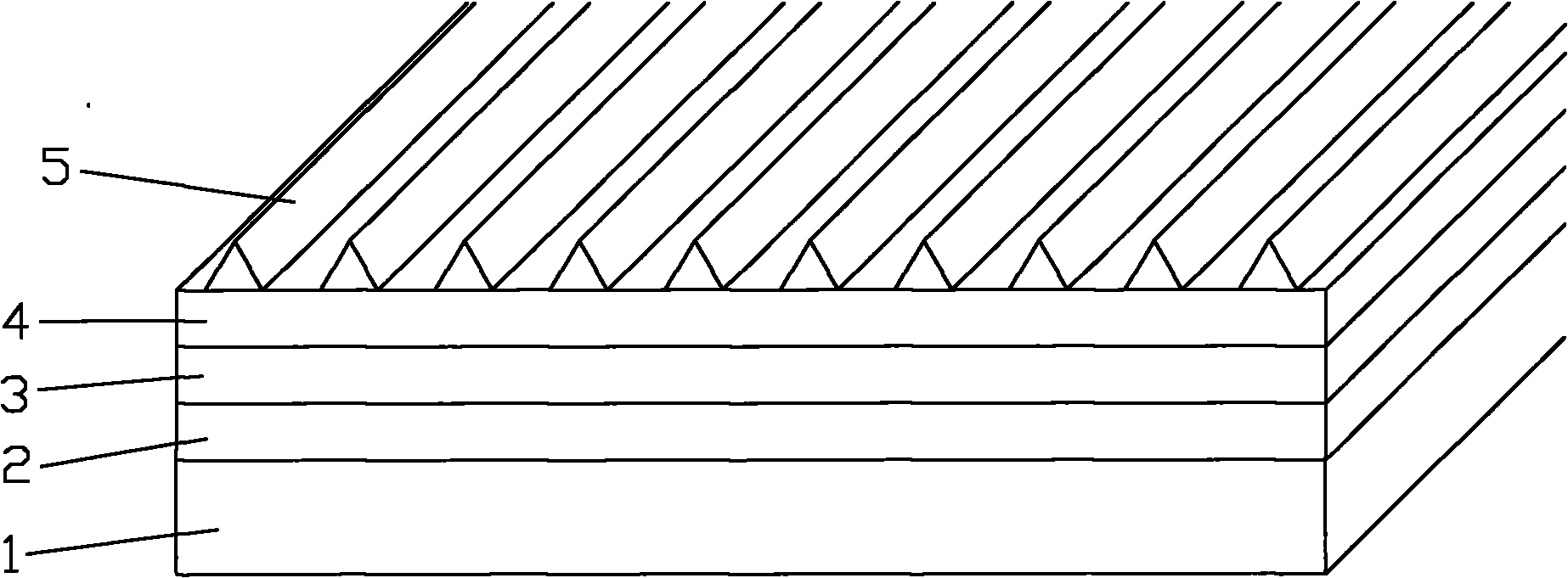
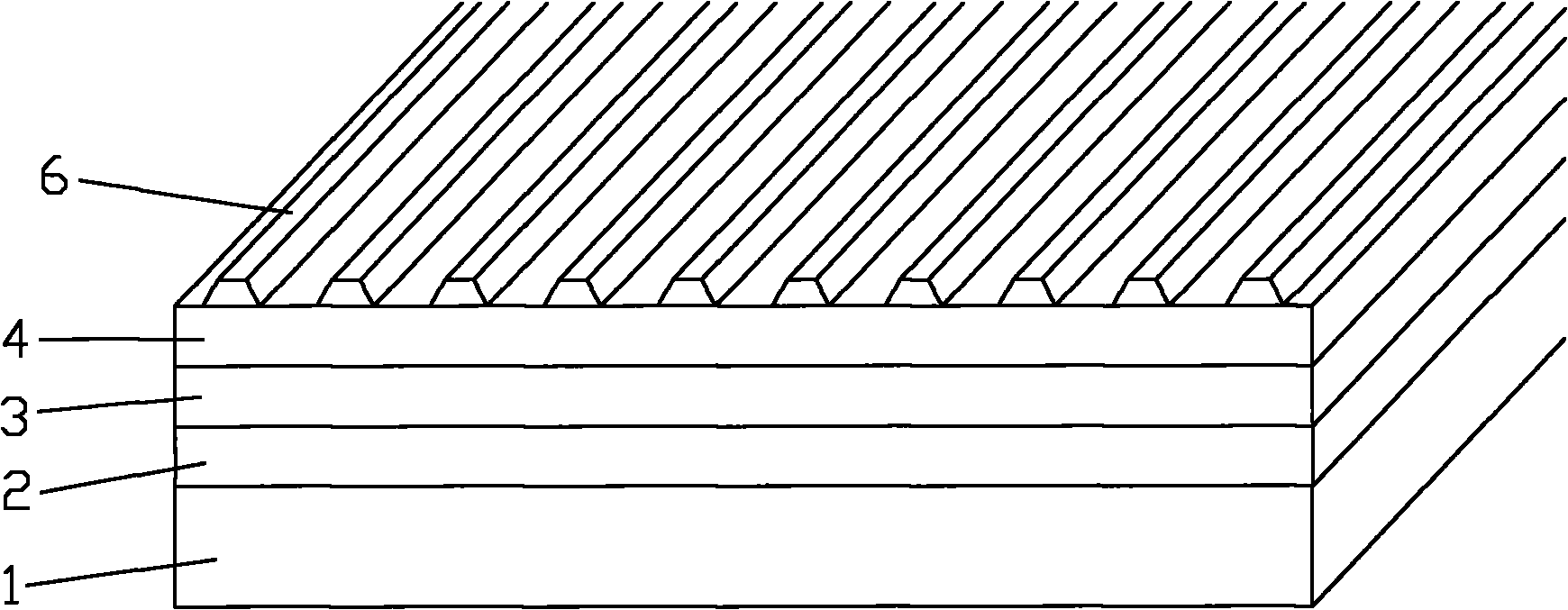
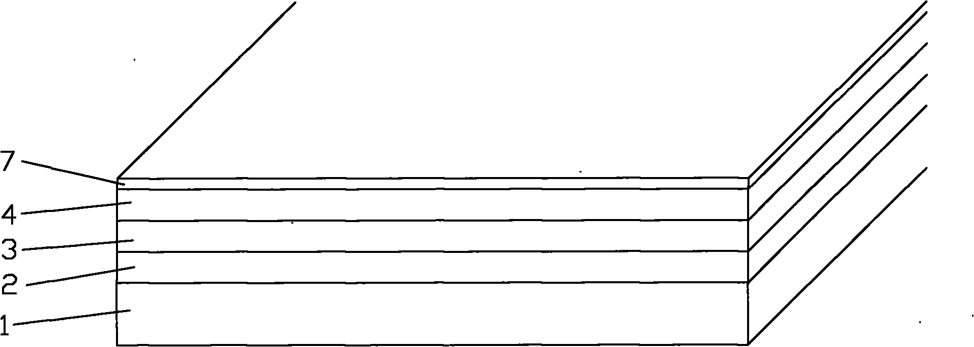
[0012] The invention discloses a light emitting diode structure, such as figure 1 with figure 2 As shown, it includes a substrate 1 and a light-emitting structure on the substrate. The light-emitting structure of the light-emitting diode includes an N-GaN layer 2, a multi-quantum well layer 3 and a P-GaN layer 4 from bottom to top. - On the GaN layer 4 there is a second epitaxial layer formed by secondary epitaxial growth, and the second epitaxial layer is a striped pyramid with a wide bottom and a narrow top.

[0013] The convex structure on the surface of the second epitaxial layer is a strip-shaped protrusion with a wide bottom and a narrow top, and the cross-section of the strip-shaped pyramid can be a triangle 5, such as figure 1 As shown, it can also be a trapezoid or a quadrilateral 6 close to a trapezoid, such as figure 2 As shown, for example, the upper and lower bases are not parallel, or the upper base is curved.

[0014] For the second epitaxial layer having a...


PUM


Abstract

The invention discloses a light-emitting diode structure. A second epitaxial layer is generated on the surface of an epitaxial structure of the light-emitting diode through a secondary epitaxy. The second epitaxial layer is of uneven pyramidal structure with certain cycle. The invention further discloses a method of manufacturing the light-emitting diode structure, which comprises steps of: manufacturing a layer of mask of periodic hollow structure on the surface of the epitaxial structure after generating the original epitaxial structure of the light-emitting diode, then conducting epitaxial growth again at the hollow position of the mask, i.e., on the exposed surface of the epitaxial structure by re-growth technology to obtain the second epitaxial layer. The structure and the method increase the light emitting efficiency while changing the light emitting angle of the light-emitting diode, and increase the uniformity and brightness of the light from the light-emitting diode. The structure and the method increase the coupling efficiency of a light guide plate, improve the brightness of a panel and ensure the uniformity of panel brightness.

Description

technical field [0001] The invention relates to a structure of a semiconductor device, in particular to a structure of a light emitting diode. The invention also relates to a manufacturing method of a semiconductor device, especially a manufacturing method of a light emitting diode. Background technique [0002] Existing light-emitting diodes have a roughened layer on the light-emitting structure, and the surface of the roughened layer will have many depressions. Because of the surface of these depressions, the light generated by the light-emitting diode will be avoided when it is emitted from the surface of the device. The total reflection causes the loss of luminous power and reduces the light extraction efficiency of the device. The existing roughening layer of light-emitting diodes, which contains many depressions, is usually made by growing a roughening layer at a relatively low temperature after the light-emitting structure is grown. Due to the low temperature, the cr...

Claims


Application Information

Patent Timeline
Patent Type & Authority Applications(China)
IPC IPC(8): H01L33/00
Inventor 郝茂盛周健华张楠陈诚潘尧波袁根如李士涛
Owner EPILIGHT TECH
Why Eureka
Try Eureka