

Method for analyzing masks for photolithography
A technology of mask plate and lithography, which is applied in the field of analysis of mask plates used in lithography, and can solve problems such as complex evaluation
- Summary
- Abstract
- Description
- Claims
- Application Information
AI Technical Summary
Problems solved by technology
Method used
Image

Examples
Embodiment Construction
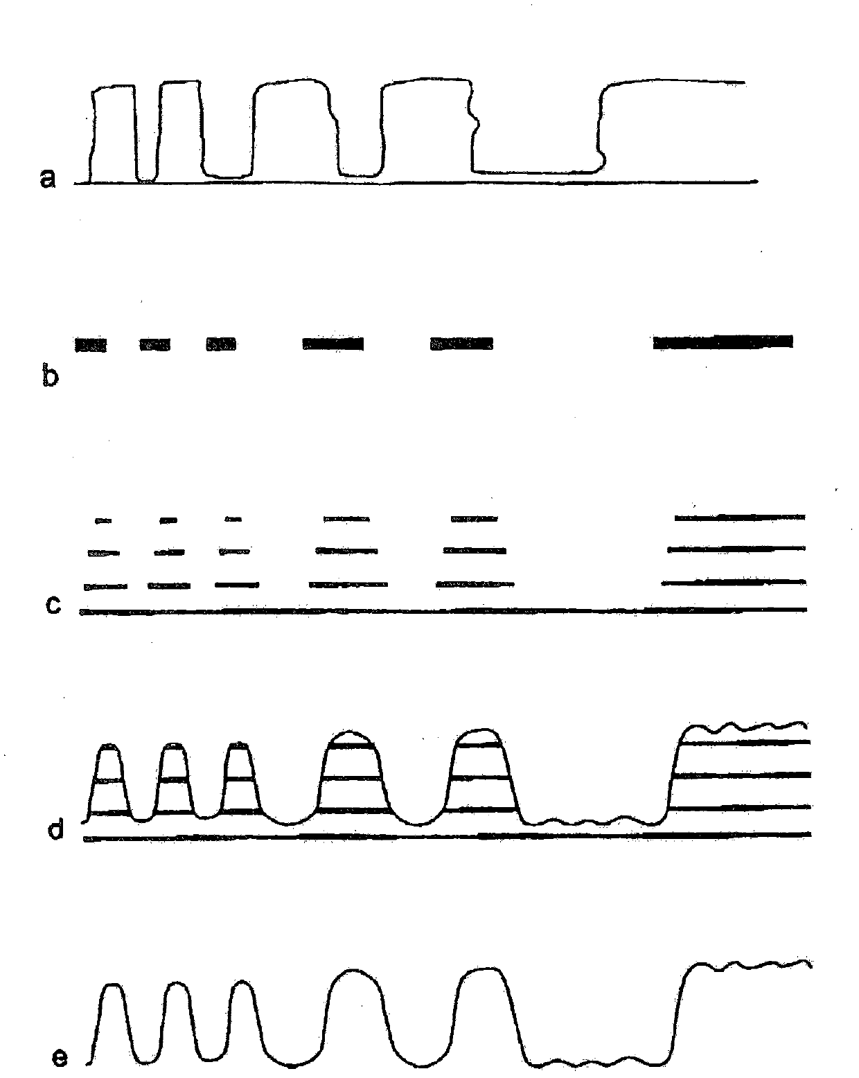
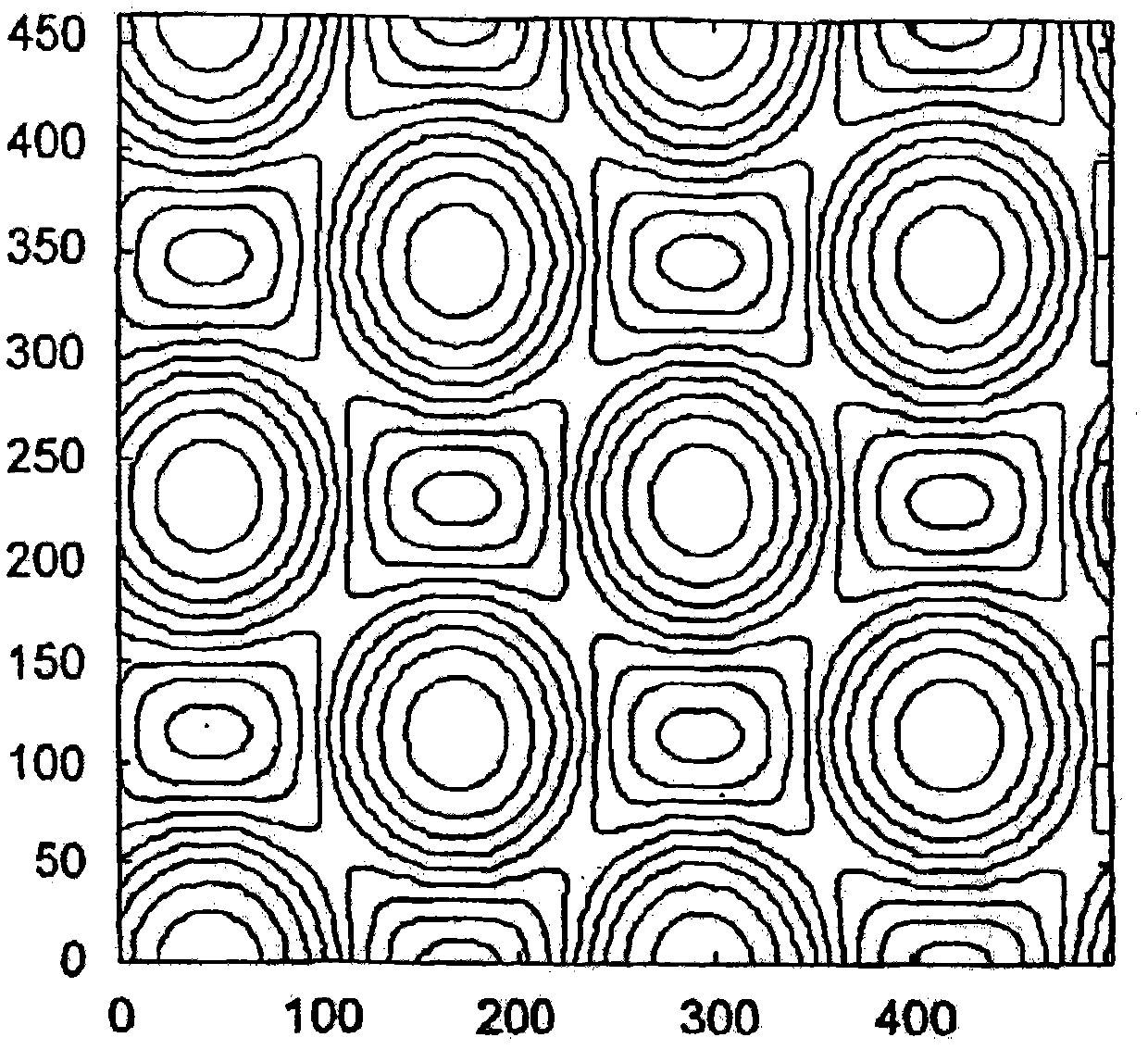
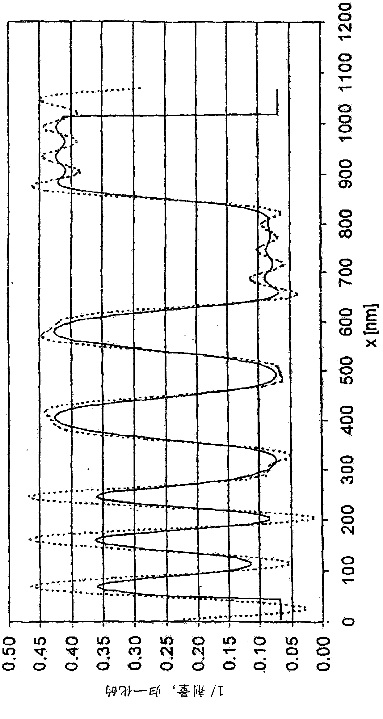
[0030] In a method of analyzing a reticle for lithography, a first step involves recording an aerial image of the reticle at a focus setting. In this case, the focal point is set in a plane that is actually located in the area of the photoresist layer applied to the wafer. Subsequently, the images are digitized and stored in spatial image data records. This spatial image data record is then transferred to an algorithm that simulates the exposure of a lithographic wafer. Exposure and development of a photoresist layer having a predetermined thickness applied to the surface of the wafer is simulated according to predetermined parameters such as energy dose (ie, energy input per unit area). In this case, the aerial image data record defines those locations on the photoresist layer on which light falls and those locations on which light does not shine. Exposure and development are then simulated depending on the type of photoresist. In the case of a positive photoresist, this...
PUM
 Abstract
Description
Claims
Application Information