Semiconductor light-emitting device with double-sided passivation
一种发光器件、半导体的技术,应用在半导体器件、半导体/固态器件制造、半导体/固态器件零部件等方向,能够解决增加反向漏电流量、降低LED效率和稳定性、增大表面复合率等问题
- Summary
- Abstract
- Description
- Claims
- Application Information
AI Technical Summary
Problems solved by technology
Method used
Image

Examples
specific Embodiment
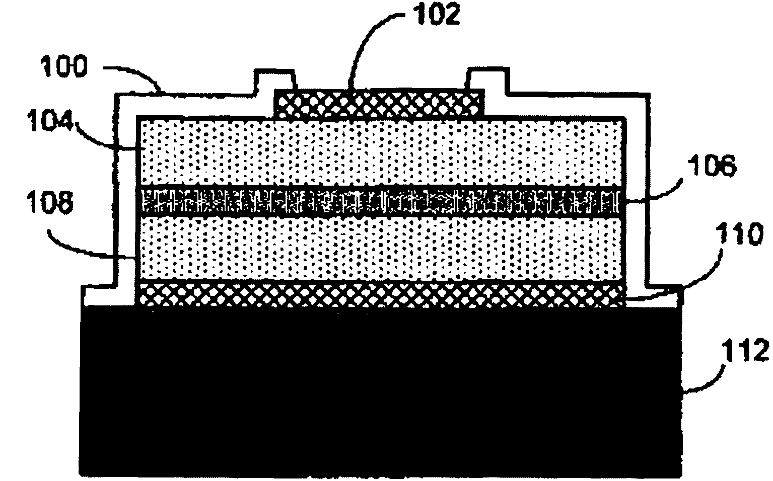
[0038] In one embodiment, the conventional substrate is patterned and etched to form an independent mesa. The size of each table is about 300×300μm 2 . The lower passivation layer is made of 500 angstroms thick SiO 2 Layer is formed, and the upper passivation layer is made of 2000 angstroms thick SiO 2 Layer formation. After etching, the size of the p-side electrode is about 250×250μm 2 . The upper surface area of the device after removing the edges is about 280×280μm 2 .
[0039] In one embodiment, the size of each mesa is approximately 300×300μm 2 . The lower passivation layer is made of 500 angstroms thick SiO 2 Layer is formed, and the upper passivation layer is made of 2000 angstroms thick SiN x Layer formation. After etching, the size of the p-side electrode is about 250×250μm 2 . The area of the upper surface of the device after removing the edges is about 280×280μm 2 .
[0040] In one embodiment, the size of each mesa is approximately 300×300μm 2 , The lower passiv...
PUM
 Abstract
Description
Claims
Application Information
 - R&D
- Intellectual Property
- Life Sciences
- Materials
- Tech Scout
- Unparalleled Data Quality
- Higher Quality Content
- 60% Fewer Hallucinations
Browse by: Latest US Patents, China's latest patents, Technical Efficacy Thesaurus, Application Domain, Technology Topic, Popular Technical Reports.
© 2025 PatSnap. All rights reserved.Legal|Privacy policy|Modern Slavery Act Transparency Statement|Sitemap|About US| Contact US: help@patsnap.com