An apparatus, a method for establishing a conductive pattern on a planar insulating substrate, the planar insulating substrate and a chipset thereof

A technology of insulating substrates and conductive planes, applied in the direction of conductive pattern formation, electrographic pattern formation, patterning and photolithography, etc., can solve the problems of non-customization, time-consuming steps, high temperature, etc.

Active Publication Date: 2011-04-13
DIGITAL TAGS FINLAND OY
View PDF0 Cites 5 Cited by
  • Summary
  • Abstract
  • Description
  • Claims
  • Application Information

AI Technical Summary

Problems solved by technology

Removal of diluents or adjuvants originally included in components requires time-consuming steps
[0005] The above known methods have some restrictions on the substrates that can be used in these known methods
None of these methods are well suited to paper, fibreboard, board-like substrates or the like due to the very high temperatures used or to weakening the locally compressed substrate
On the other hand, deposition masks, stencils, or screens are not ideally fast, uncustomizable, and inflexible because they unnecessarily complicate the deposition process and limit the available resolution

Method used


Image

  • An apparatus, a method for establishing a conductive pattern on a planar insulating substrate, the planar insulating substrate and a chipset thereof
  • An apparatus, a method for establishing a conductive pattern on a planar insulating substrate, the planar insulating substrate and a chipset thereof
  • An apparatus, a method for establishing a conductive pattern on a planar insulating substrate, the planar insulating substrate and a chipset thereof

Examples


Embodiment Construction

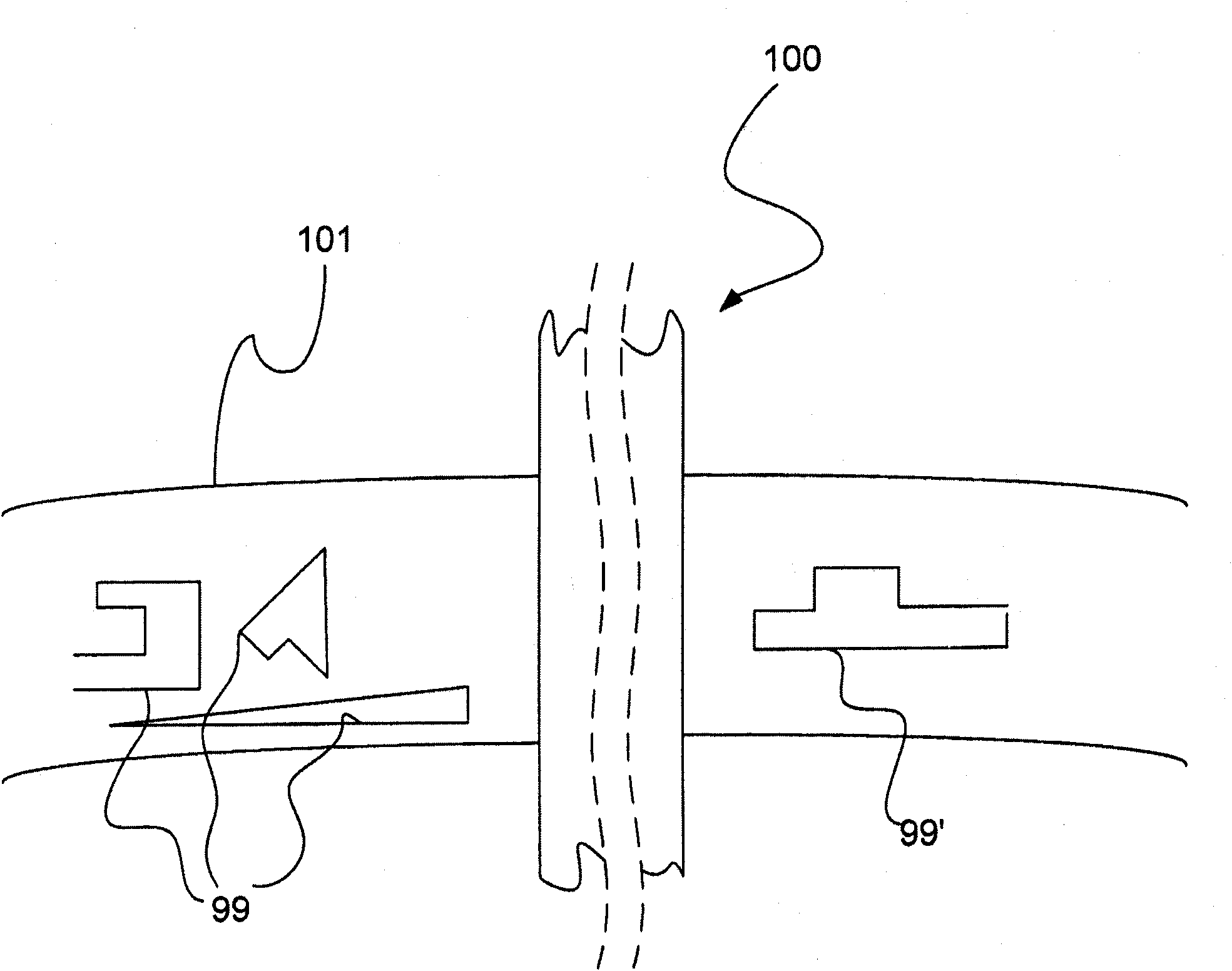
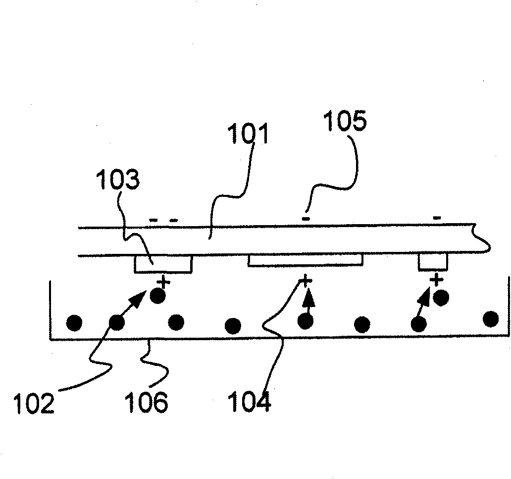
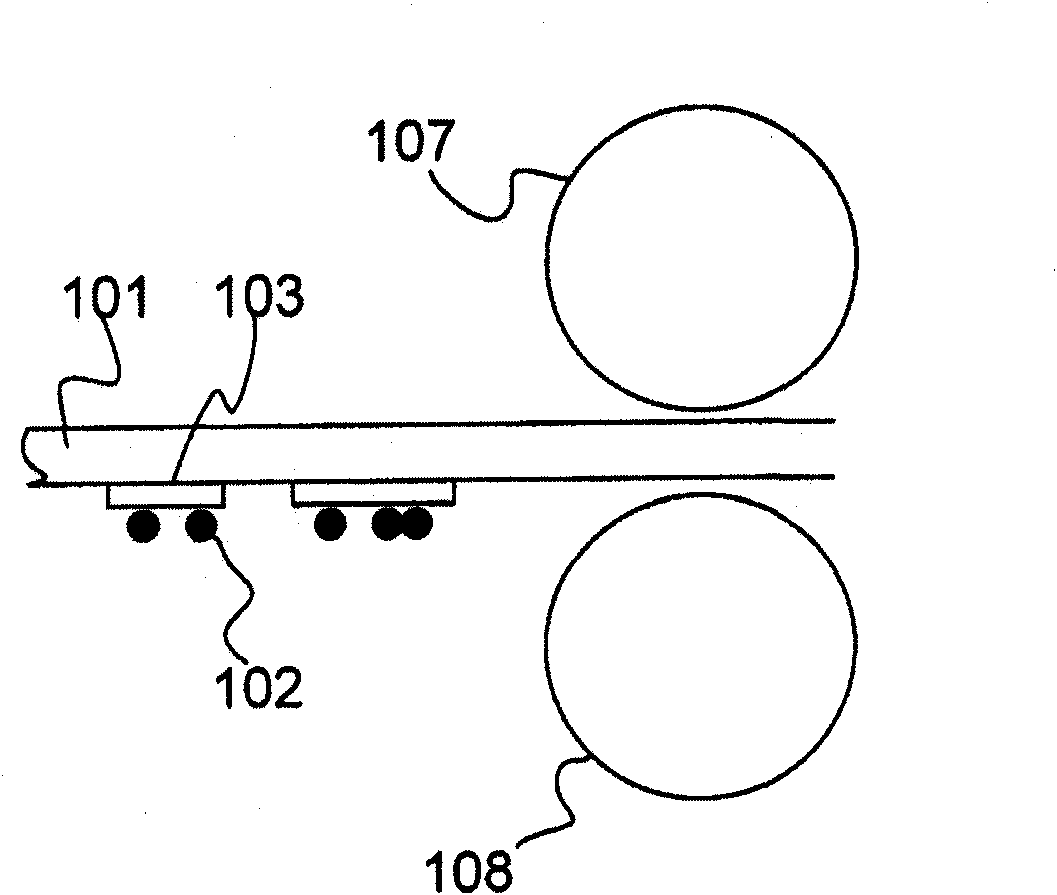
[0033] figure 1 A general view of a portion of a device 100 configured to form a conductive pattern 99 on a flat insulating substrate 101 is shown, wherein the pattern 99 is shown, in accordance with an embodiment of the present invention. Various embodiments of the invention are based on (micro)particles 102 (in figure 1 ), the particles can be deposited and permanently attached to various substrates 101 while increasing the conductivity of the pattern 99 being deposited. This can be obtained by means of at least one module of the device 100 configured to form a predetermined pattern 99 on the flat insulating substrate 101 so that the conductive particles 102 can gather according to the predetermined pattern 99 . Furthermore, at least one further module of the device 100 is configured to transfer the conductive particles to the flat insulating substrate 101, wherein the conductive particles 102 are arranged to aggregate according to a predetermined pattern. Furthermore, the...


PUM

PropertyMeasurementUnit
melting pointaaaaaaaaaa

Abstract

An apparatus, a method, a planar insulating substrate and a chipset have been presented, comprising at least one module configured to establish a predefined pattern on a planar insulating substrate so that conductive particles can gather according to the predefined pattern. At least one another module is configured to transfer the conductive particles to the planar insulating substrate, wherein the conductive particles are arranged to gather according to the predefined pattern. A sintering module is configured to fuse the conductive particles on the planar insulating substrate, wherein the conductive particles are arranged to fuse according to the predefined pattern to establish a conductive plane on the planar insulating substrate. Embodiment of the invention relate to printable or printing electronics on a fibrous web.

Description

technical field [0001] The present invention relates to an apparatus for forming a conductive pattern on a flat insulating substrate, and moreover, the present invention relates to a method for forming a conductive pattern on a flat insulating substrate. Furthermore, the present invention relates to a flat insulating substrate comprising the conductive pattern thus formed. Furthermore, the invention relates to a chip set thus formed on a flat insulating substrate. Background technique [0002] Printed electronics, especially on flexible substrates, are used for electronic components and logic solutions, disposable electronics, and even printed displays. Currently, printed electronics applications use methods familiar in conventional electronics fabrication, such as electroplating and screen printing. However, these methods are slow and not well suited to porous substrates and / or substrates in the form of fabrics. Additionally, flexo and rotogravure printing have been used...

Claims


Application Information

Patent Timeline
Patent Type & Authority Applications(China)
IPC IPC(8): H05K3/10C23C24/08C23C26/00
CPCH05K2203/0522H05K1/0393C23C26/00H05K2203/0143H05K3/1266H05K2203/1545H05K2203/0517C23C24/10H05K2203/1131Y10T428/24322Y10T428/24917Y10T428/24521Y10T428/256Y10T428/249953H05K3/10
Inventor 尤哈·麦加拉派翠·瑟维奥
Owner DIGITAL TAGS FINLAND OY
Why Eureka
Try Eureka