Multilayer chip varistor and manufacturing method thereof

A varistor, multi-layer chip technology, applied in the direction of resistance manufacturing, varistors, resistors, etc., can solve the problems of circuit complexity, multi-line area, circuit design, maintenance hidden dangers, etc., to save installation space, The effect of reducing the size of the component

Inactive Publication Date: 2011-04-20
SHENZHEN SUNLORD ELECTRONICS
View PDF4 Cites 10 Cited by
  • Summary
  • Abstract
  • Description
  • Claims
  • Application Information

AI Technical Summary

Problems solved by technology

Due to the increasing use of ordinary chip varistors in various circuits, especially the application of multiple varistors in the same PCB circuit, the multilayer chip varistors of the above patent have the following technical defects: often lead to Occupies too much line area and complicates the circuit, which brings hidden dangers in circuit design and maintenance

Method used


Image

  • Multilayer chip varistor and manufacturing method thereof
  • Multilayer chip varistor and manufacturing method thereof
  • Multilayer chip varistor and manufacturing method thereof

Examples


Embodiment 1

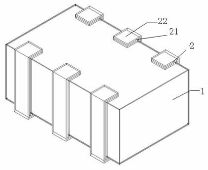
[0042] Such as Figure 1-4 As shown, the multilayer chip varistor of this embodiment includes a varistor substrate whose overall shape is a cuboid, and the varistor substrate includes a lower substrate, an upper substrate, and a substrate between the upper substrate and the lower substrate. A piezoresistor substrate consisting of multiple layers of piezoresistor units including internal electrodes and piezoresistor films. The long-height sides of the piezoresistor substrate are formed by pairwise 4, 6, or 8 terminal electrodes opposite each other. Row-shaped structure, the wide-high side of the varistor substrate has no auxiliary terminal electrodes; the internal electrodes include 2, 3 or 4 mutually independent internal electrode units, and each of the internal electrode units is connected to a pair of the Terminal connection.

[0043] The manufacturing method of the multilayer chip varistor of this embodiment includes the following steps:

[0044] (1) Preparation of slurry...

Embodiment 2

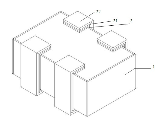
[0093] Such as Figure 5-7 As shown, the difference between the multilayer chip varistor of this embodiment and the multilayer chip varistor of Embodiment 1 is that the multilayer chip varistor of this embodiment also includes two A pair of auxiliary terminal electrodes on two wide and high sides, the auxiliary terminal electrodes are connected through internal electrodes, and form a loop with a pair of terminal electrodes connected to the same internal electrode unit. The auxiliary terminal electrode can be used as a ground connection terminal.

[0094] The manufacturing method of the multilayer chip varistor of this embodiment includes:

[0095] (1) Configure the slurry: the same as in Example 1

[0096] (2) Lamination: the manufacturing method is the same as that of Embodiment 1, the only difference lies in the design of the internal electrode pattern structure.

[0097] (3)-(8) The manufacturing method is the same as the first embodiment, the only difference is that an ...

Embodiment 3

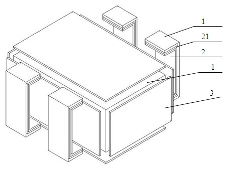
[0099] Such as Figure 8-12 As shown, the difference between the multilayer chip varistor of this embodiment and the multilayer chip varistor of Embodiment 2 is that: the multilayer chip varistor of this embodiment also includes multiple The resistance layer 6 on the upper substrate and / or the lower substrate, the two ends of each resistance layer 6 are respectively connected to a pair of terminal electrodes 2 connected to the same internal electrode unit 7; and the upper surface of the resistance layer has a layer of organic Material protective layer or inorganic material protective layer 5 cover. The resistance layer 6 is used to form an R-C loop in the varistor, so that the multilayer chip varistor of this embodiment has the function of anti-electromagnetic interference, and the protective layer 5 has insulation and waterproof functions, and is used to protect the resistance layer. Its material Preferable polymer materials, such as epoxy resin, phenolic resin and other mat...


PUM


Abstract

The invention discloses a multilayer chip varistor and a manufacturing method thereof. The varistor comprises a varistor substrate in an entirely cuboid shape; the varistor substrate comprises a lower base plate, an upper base plate and a varistor substrate; the varistor substrate is arranged between the upper base plate and the lower base plate and formed by stacking multiple varistor units each of which comprises an inner electrode and a varistor film; the varistor also comprises at least two pairs of end electrodes; each pair of end electrodes is oppositely arranged on the two long-high side surfaces of the varistor substrate; the inner electrode comprises at least two inner electrode units; and each inner electrode unit is connected with a pair of end electrodes respectively. The method is used for manufacturing the varistor. The invention has the following beneficial effects: multiple varistor units with independent functions are integrated, the element volume is reduced, and the varistor mounting space is saved.

Description

technical field [0001] The invention relates to a varistor, in particular to a multilayer chip varistor and a manufacturing method thereof. The contents disclosed in the applicant's previous Chinese patent application No. CN1909122A are incorporated herein by reference. Background technique [0002] The Chinese patent application document "Multilayer chip varistor and its manufacturing method" with publication number CN1909122A discloses a varistor with high safety, convenient use and low cost and its manufacturing method. [0003] However, with the rapid development of electronic information systems, chip varistor components have been widely used, and more and more components have achieved chip and miniaturization. Due to the increasing use of ordinary chip varistors in various circuits, especially the application of multiple varistors in the same PCB circuit, the multilayer chip varistors of the above patent have the following technical defects: often lead to Occupying t...

Claims


Application Information

Patent Timeline
Patent Type & Authority Applications(China)
IPC IPC(8): H01C7/10H01C1/06H01C1/14H01C17/00
Inventor 师习恩贾广平冯志刚
Owner SHENZHEN SUNLORD ELECTRONICS
Why Eureka
Try Eureka