Printed circuit board, method and device for detecting layer-to-layer registration of circuit graphs at two surfaces thereof

A circuit pattern and alignment technology, which is applied in the direction of measuring devices, printed circuits, printed circuit manufacturing, etc., can solve the problem that the core board is difficult to see the misalignment inspection ring, and detect whether the alignment between the circuit graphics layers on both sides of the core board is Meet the requirements and other issues to achieve the effect of improving the detection accuracy

Active Publication Date: 2011-04-27
NEW FOUNDER HLDG DEV LLC +1
View PDF6 Cites 17 Cited by
  • Summary
  • Abstract
  • Description
  • Claims
  • Application Information

AI Technical Summary

Problems solved by technology

[0004] With the development of the printed circuit board industry, the production of printed circuit boards is developing in the direction of high multi-layer, high precision, and miniaturization. The specific value of the interlayer offset between the two layers of the circuit pattern of the core board, which cannot be satisfied by the dislocation r

Method used


Image

  • Printed circuit board, method and device for detecting layer-to-layer registration of circuit graphs at two surfaces thereof
  • Printed circuit board, method and device for detecting layer-to-layer registration of circuit graphs at two surfaces thereof
  • Printed circuit board, method and device for detecting layer-to-layer registration of circuit graphs at two surfaces thereof

Examples


Embodiment 1

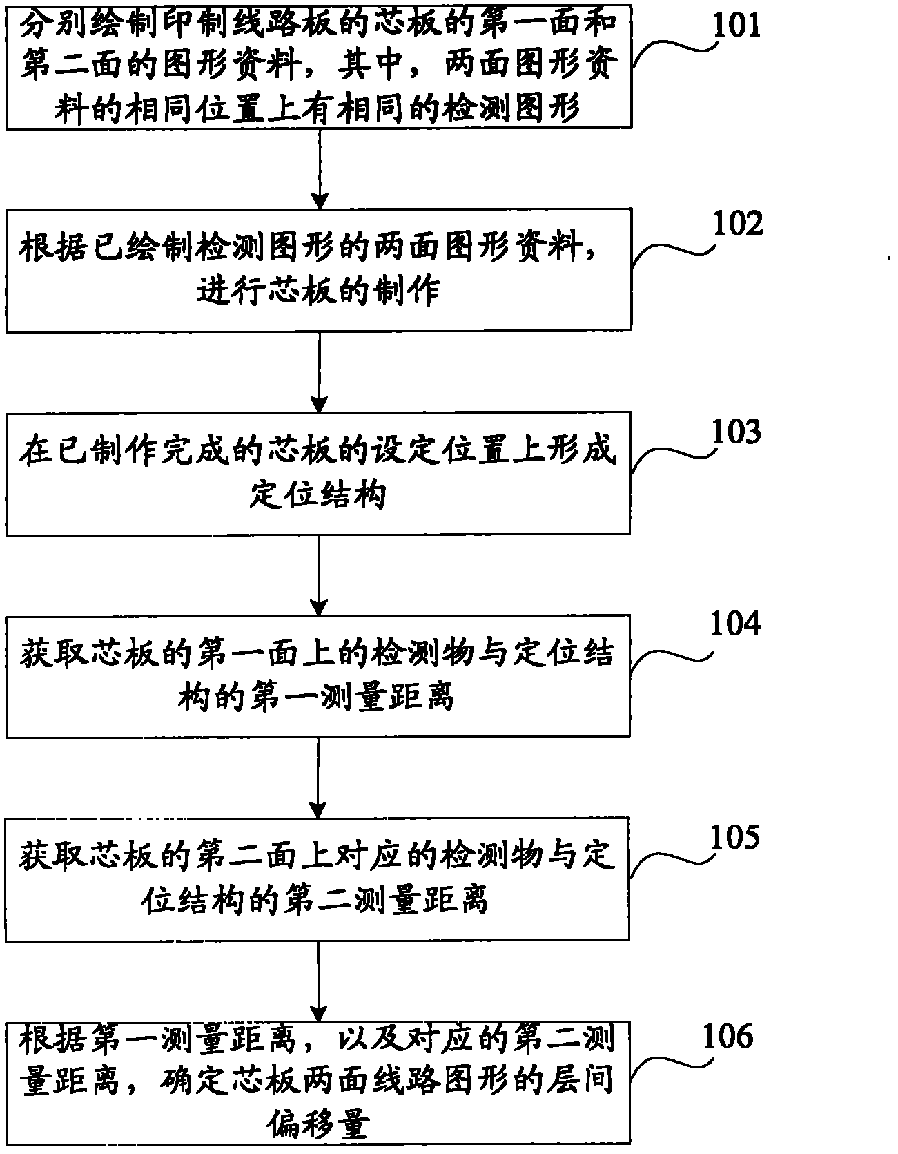
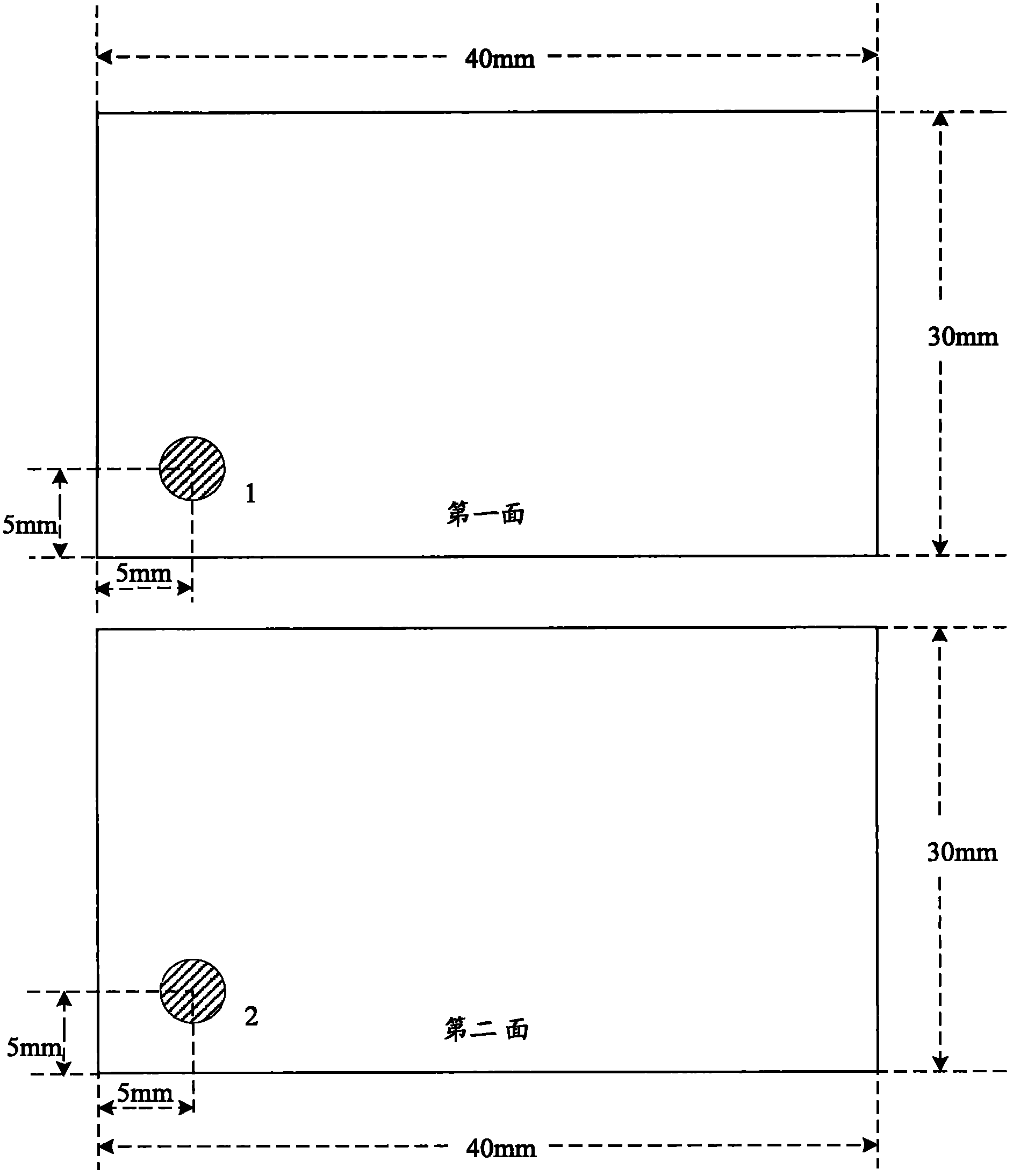
[0066] Embodiment 1. In this embodiment, the core board of the printed circuit board includes a double-sided circuit pattern. The shape of the core board is a regular rectangle. There is only one detection pattern on the graphic data of each side of the core board, and the detection pattern is circle, in this embodiment, the process of detecting the interlayer alignment of the circuit patterns on both sides of the printed circuit board is as follows: Figure 4 shown, including:

[0067] Step 401: Draw a circle with a set size at the same position on the upper left corner of the graphic data on both sides of the core board of the printed circuit board.

[0068] In this embodiment, the graphics data of the designed core board are as follows: Figure 5 As shown, there is a circle 1 with a diameter of 4.0mm in the upper left corner of the graphic data on the first surface, and the center origin of the circle 1 is 6.0mm and 4.0mm from the left side and the top side of the first su...

Embodiment 2

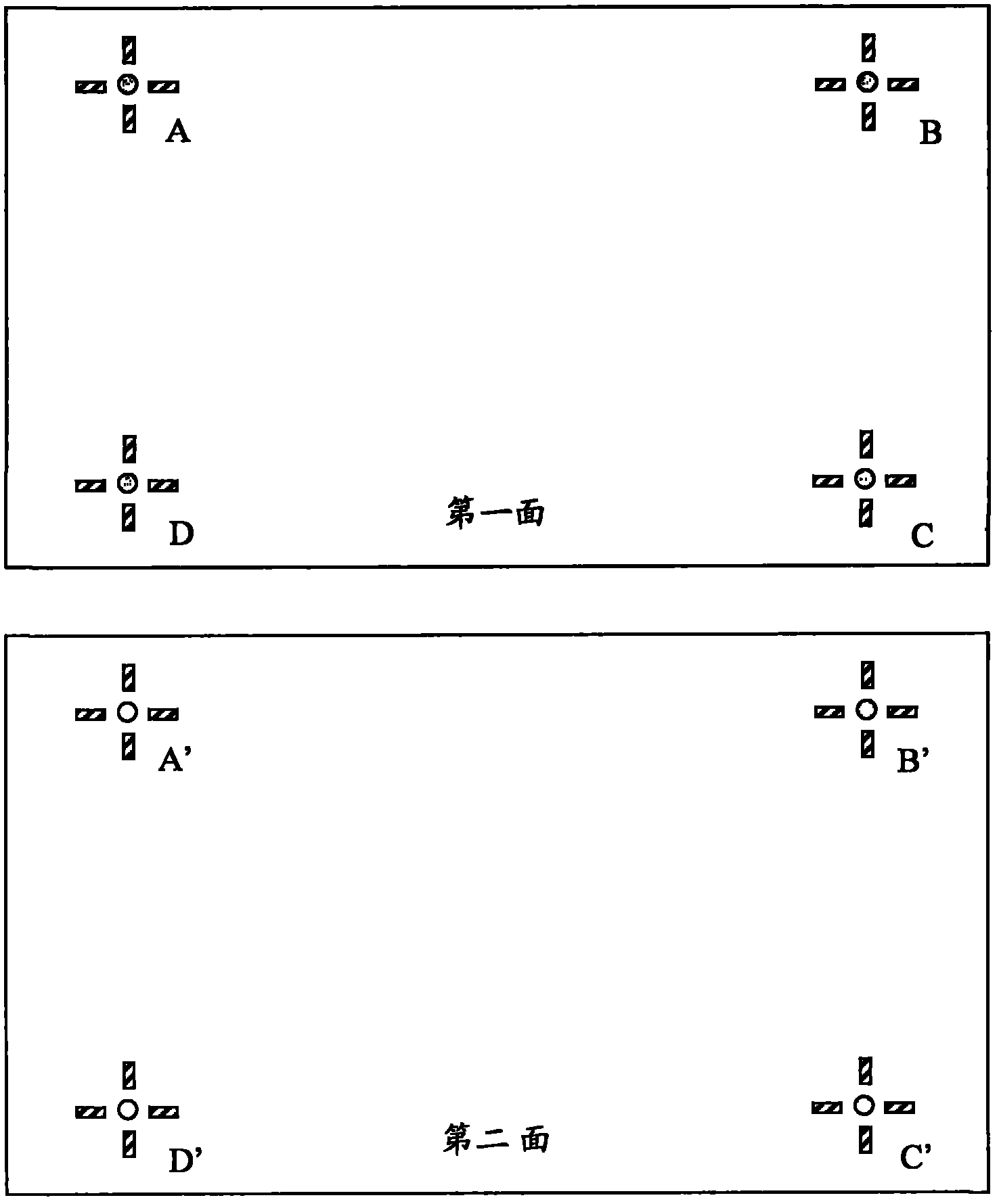
[0082] Embodiment two, in the present embodiment, core plate comprises double-sided circuit pattern, and the profile of core plate is an irregular quadrilateral, and there are four detection patterns on the figure data of every side, and each detection pattern is target disk shape, Then in this embodiment, the process of detecting the interlayer alignment of the circuit patterns on both sides of the core board is as follows: Figure 7 shown, including:


PUM


Abstract

The invention discloses a method for detecting layer-to-layer registration of circuit graphs at the two surfaces of a core board, which is used for improving the detecting precision of layer-to-layer registration of the circuit graphs at the two surfaces of the core board of the existing printed circuit board. The method comprises the following steps: graphic data is respectively drawn on a firstsurface and a second surface of the core board of the printed circuit board, wherein the same positions of the graphic data of the first surface and the second surface are respectively drawn with a detecting graph, the core board is manufactured according to the graphic data of the first surface and the second surface on which the detecting graphs are drawn, wherein the manufactured core board comprises a detected object corresponding to the position of each detecting graph, a positioning structure is formed on a set position of the manufactured core board; and the layer-to-layer offset of the circuit graphs at the two surfaces of the core board is determined according to the measured distance from the detected objects on the first surface and the second surface of the core board to the positioning structure. The invention also discloses a printed circuit board and a device for detecting layer-to-layer registration of circuit graphs at the two surfaces of the core board.

Description

technical field [0001] The invention relates to the technical field of printed circuit boards, in particular to a method, a device and a printed circuit board for detecting the interlayer alignment of circuit patterns on both sides of a core board in a printed circuit board. Background technique [0002] The production of printed circuit boards usually starts with the production of core board graphics, and the interlayer alignment of the circuit graphics on both sides of the core board is very important for subsequent processing, especially in multi-core boards that are pressed together by multiple core boards. In the production of multi-layer printed circuit boards, the requirements for inter-layer alignment of circuit patterns on both sides of the core board are more stringent. If the interlayer offset of the graphics on both sides of the core board exceeds a certain level, the electrical performance of the electroplated copper connecting the two-layer graphics lines will ...

Claims


Application Information

Patent Timeline
IPC IPC(8): G01B21/02H05K3/00
Inventor 唐国梁
Owner NEW FOUNDER HLDG DEV LLC
Why Eureka
Try Eureka