Fringe field switching mode liquid crystal display device and method of fabricating the same

A mode and substrate technology, applied in semiconductor/solid-state device manufacturing, optics, instruments, etc., can solve problems such as increase, image quality reduction, and voltage retention rate reduction.

Inactive Publication Date: 2011-04-27
HYDIS TECH CO LTD
View PDF10 Cites 33 Cited by
  • Summary
  • Abstract
  • Description
  • Claims
  • Application Information

AI Technical Summary

Problems solved by technology

This eventually causes problems such as increased pixel voltage ΔVp, lowered voltage retention ratio (VHR), lowered image quality (e.g., afterimage or flicker), lowered transmittance, etc.

Method used


Image

  • Fringe field switching mode liquid crystal display device and method of fabricating the same
  • Fringe field switching mode liquid crystal display device and method of fabricating the same
  • Fringe field switching mode liquid crystal display device and method of fabricating the same

Examples


no. 1 example Embodiment

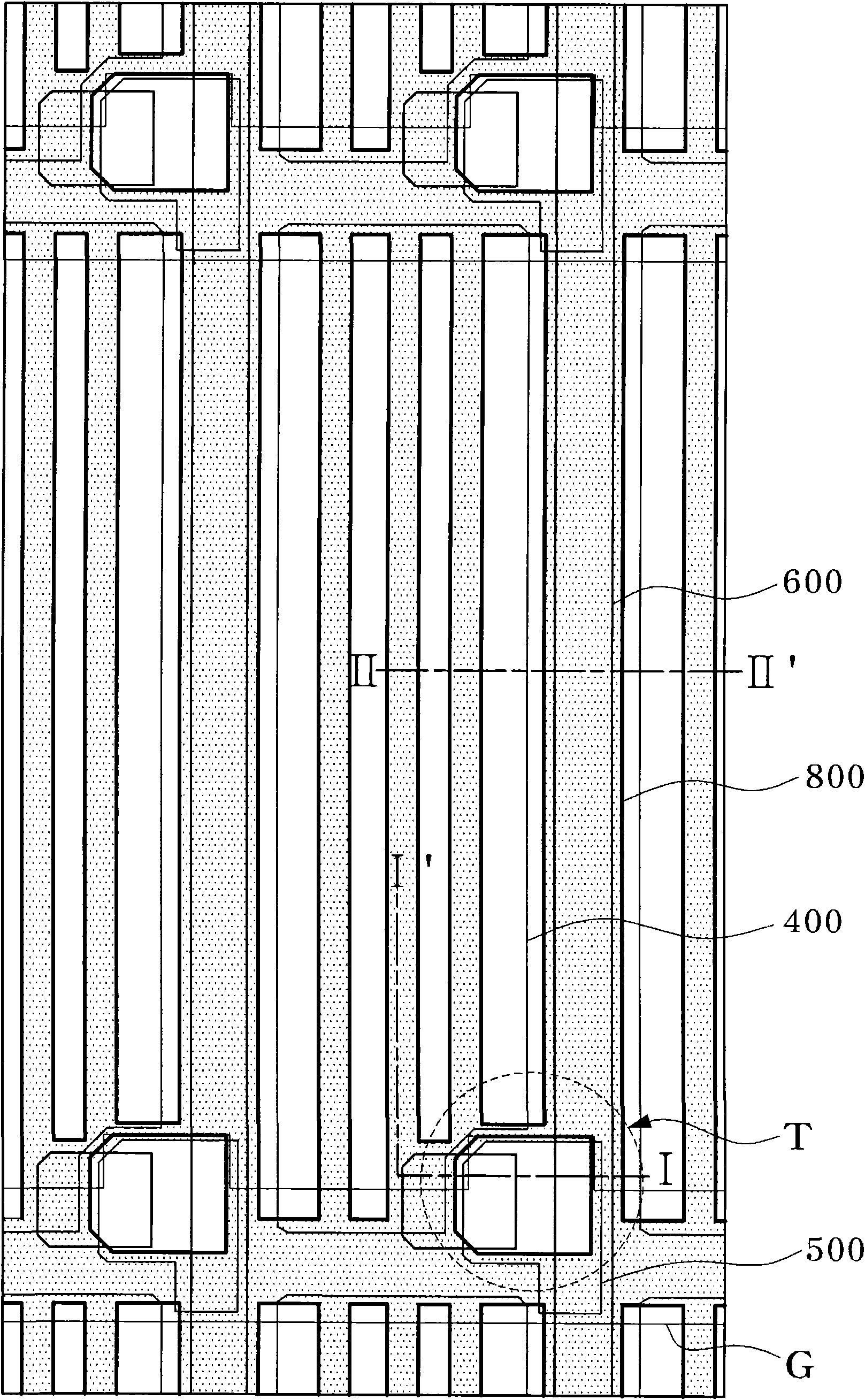
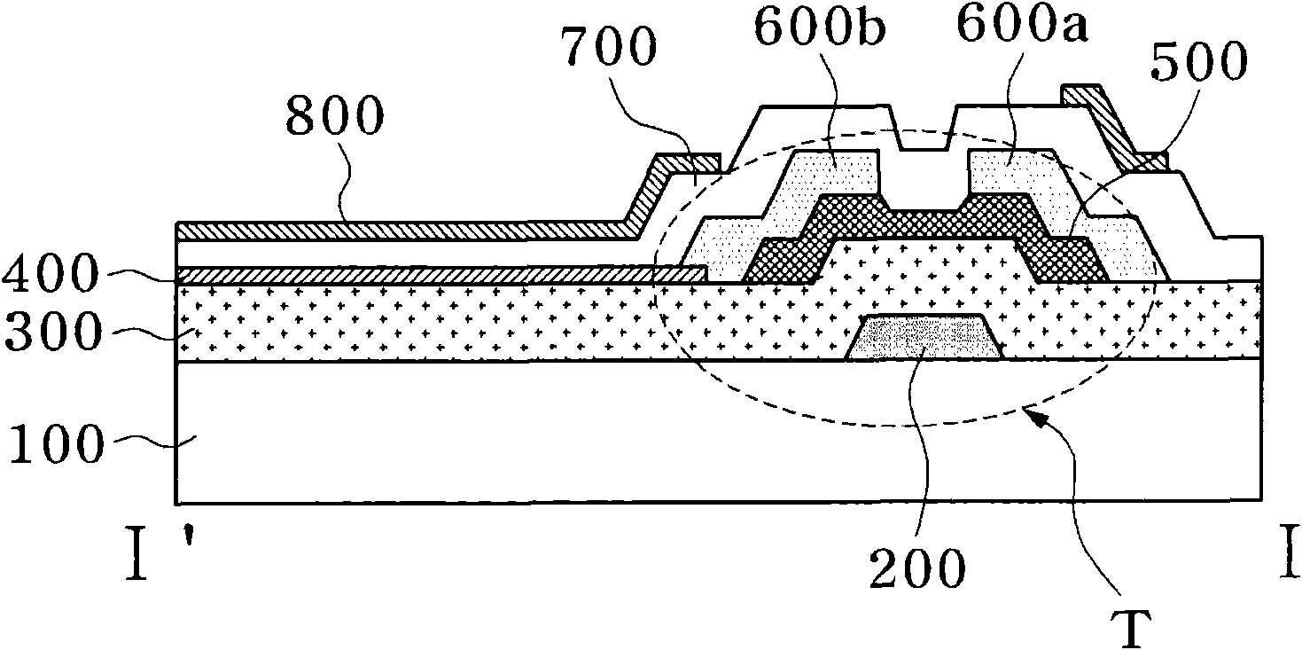
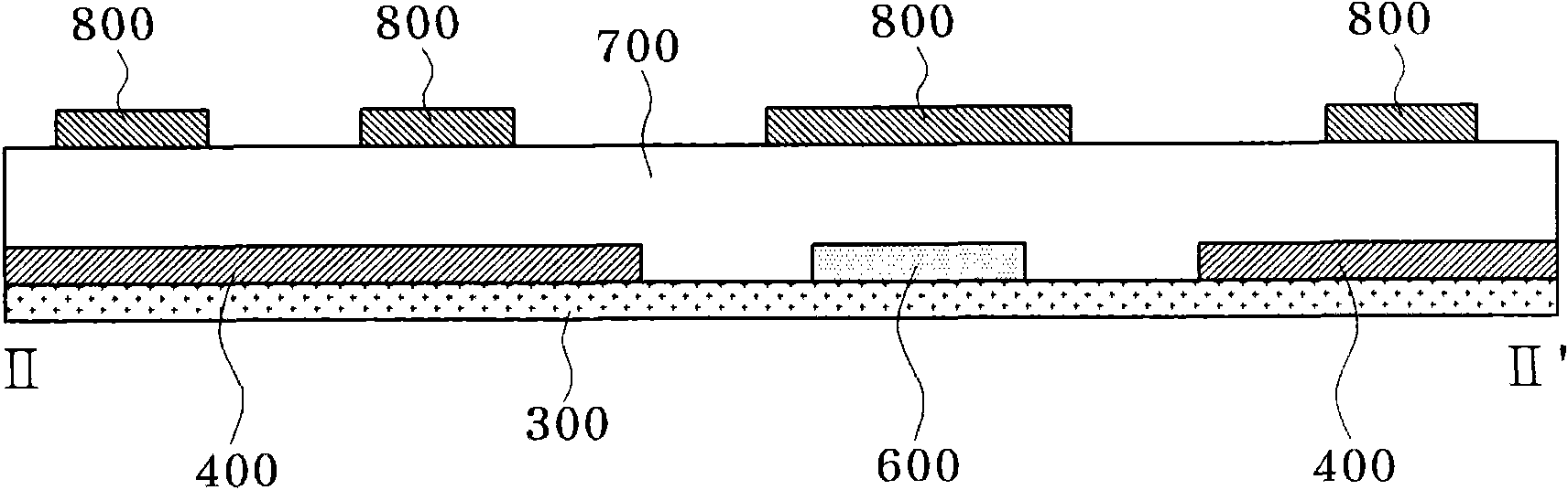
[0050] Figure 4 is a plan view of a part of the pixel region of the lower substrate of the FFS mode LCD according to the first exemplary embodiment of the present invention; Figure 5 to Figure 8 Formed for sequential display Figure 4 A plan view of the various layers shown and steps for overlapping the layers; Figure 9 for Figure 4 The sectional view taken along the line A-A'; Figure 10 for Figure 4 The sectional view taken along the line B-B'; Figure 11 is the plan view of FFS mode LCD, which shows Figure 4 part of the layer shown; Figure 12 for Figure 11 The sectional view taken along the line C-C'; Figure 13 is an equivalent circuit diagram showing a liquid crystal cell of an FFS mode LCD according to a first exemplary embodiment of the present invention.

[0051] see Figure 4 to Figure 13 , the lower substrate applied to the first exemplary embodiment of the present invention has a structure in which gate lines G and data lines 600 formed of an opaqu...

no. 2 example Embodiment

[0077] Figure 15 is a plan view of a part of a pixel region of a lower substrate of an FFS mode LCD according to a second exemplary embodiment of the present invention; Figure 16 to Figure 21 is a plan view sequentially showing the steps of forming the layers and overlapping the layers; Figure 32 for Figure 15 The cross-sectional view taken along the line D-D'.

[0078] The structure of the lower substrate applied to the second exemplary embodiment of the present invention is similar to the structure of the lower substrate applied to the above-mentioned first exemplary embodiment, for the convenience of explanation, for the same elements as in the first exemplary embodiment, The same reference numerals and names as in the first exemplary embodiment will be used.

[0079] Furthermore, the main explanation will be related to Figure 4 The difference of the lower substrate of the FFS mode LCD according to the first exemplary embodiment of the present invention is shown, t...

no. 3 example Embodiment

[0094] Figure 22 is a plan view of a part of a pixel region of a lower substrate of an FFS mode LCD according to a third exemplary embodiment of the present invention, Figure 33 then Figure 22 Sectional view taken along the line E-E' of .

[0095] see Figure 22 and Figure 33 , comparing the lower substrate of the FFS mode LCD device according to the third exemplary embodiment of the present invention with the lower substrate of the FFS mode LCD device according to the second exemplary embodiment of the present invention described above, the difference is only in the The arrangement position of the common line 900 which reduces the resistance, and the FFS mode LCD device according to the third exemplary embodiment of the present invention is the same as that of the FFS mode LCD device according to the second exemplary embodiment of the present invention in structure and its manufacturing method. Therefore, for its detailed description, refer to the second exemplary emb...


PUM


Abstract

Provided is a fringe field switching (FFS) mode liquid crystal display device (LCD) and a method of fabricating the same that are capable of effectively improving image quality by reducing loads of gate lines and data lines and increasing a conventional storage capacitance. The LCD includes a lower substrate, an upper substrate, and a liquid crystal layer disposed between the substrates, the lower substrate including unit pixel regions defined by gate lines and data lines formed to intersect each other and switching devices disposed on intersections of the gate and data lines, the LCD also comprises: a transparent pixel electrode disposed in the pixel region and a transparent common electrode spaced apart from and overlapping the transparent pixel electrode in a predetermined region with an insulating layer interposed therebetween, and a transparent auxiliary capacitive electrode spaced apart from and overlapping the transparent pixel electrode in a predetermined region with the gate insulating layer interposed therebetween, wherein the transparent auxiliary capacitive electrode is electrically connected to a common bus line formed on a non-display region of an outer periphery of the lower substrate through a contact hole, and the common bus line is connected to the transparent common electrode.

Description

[0001] Related Application Cross Reference [0002] This application claims the priority of Korean Patent Application No. 2009-95554 filed on October 8, 2009 and Korean Patent Application No. 2010-54267 filed on June 9, 2010, the contents disclosed in these two Korean Patent Applications Incorporated herein by reference in its entirety. technical field [0003] The present invention relates to an FFS (Fringe Field Switching, fringe field switching) mode LCD (Liquid Crystal Display Device, liquid crystal display device) and a manufacturing method thereof, more specifically, relates to a method for reducing the number of gate lines and data lines An FFS mode LCD capable of effectively improving image quality by loading and increasing a conventional storage capacitor Cst and a manufacturing method thereof. Background technique [0004] In general, to improve the low aperture ratio and transmittance of In-Plane Switching (IPS) mode LCD, an FFS mode LCD has been proposed, and th...

Claims


Application Information

Patent Timeline
Patent Type & Authority Applications(China)
IPC IPC(8): G02F1/1343G02F1/1362G02F1/1333H01L21/77
CPCH01L27/0207G02F1/134363G02F2001/134372H01L27/12H01L27/13G02F1/136213H01L27/1255G02F1/134372
Inventor 田旼暻金戊瑽
Owner HYDIS TECH CO LTD
Why Eureka
Try Eureka