Semiconductor flip chip package

一种倒装芯片、半导体的技术,应用在半导体器件、半导体/固态器件零部件、电固体器件等方向,能够解决不同裸晶版本、倒装芯片封装成本高、没有办法改变或是重做等问题,达到灵活成本的效果

Inactive Publication Date: 2011-04-27
MEDIATEK INC
View PDF9 Cites 4 Cited by
  • Summary
  • Abstract
  • Description
  • Claims
  • Application Information

AI Technical Summary

Problems solved by technology

[0005] The high cost of the flip-chip package described above is partly due to the need for a different bump mask for each bump option
Additionally, IC design houses often encounter nasty die revision management issues when keeping flip-chip die in stock
This is because different bump choices result in different die versions
Due to the nature of flip chip packaging, once the bump selection is utilized and the die version is determined, there is no way to change or redo it

Method used


Image

  • Semiconductor flip chip package
  • Semiconductor flip chip package
  • Semiconductor flip chip package

Examples


Embodiment Construction

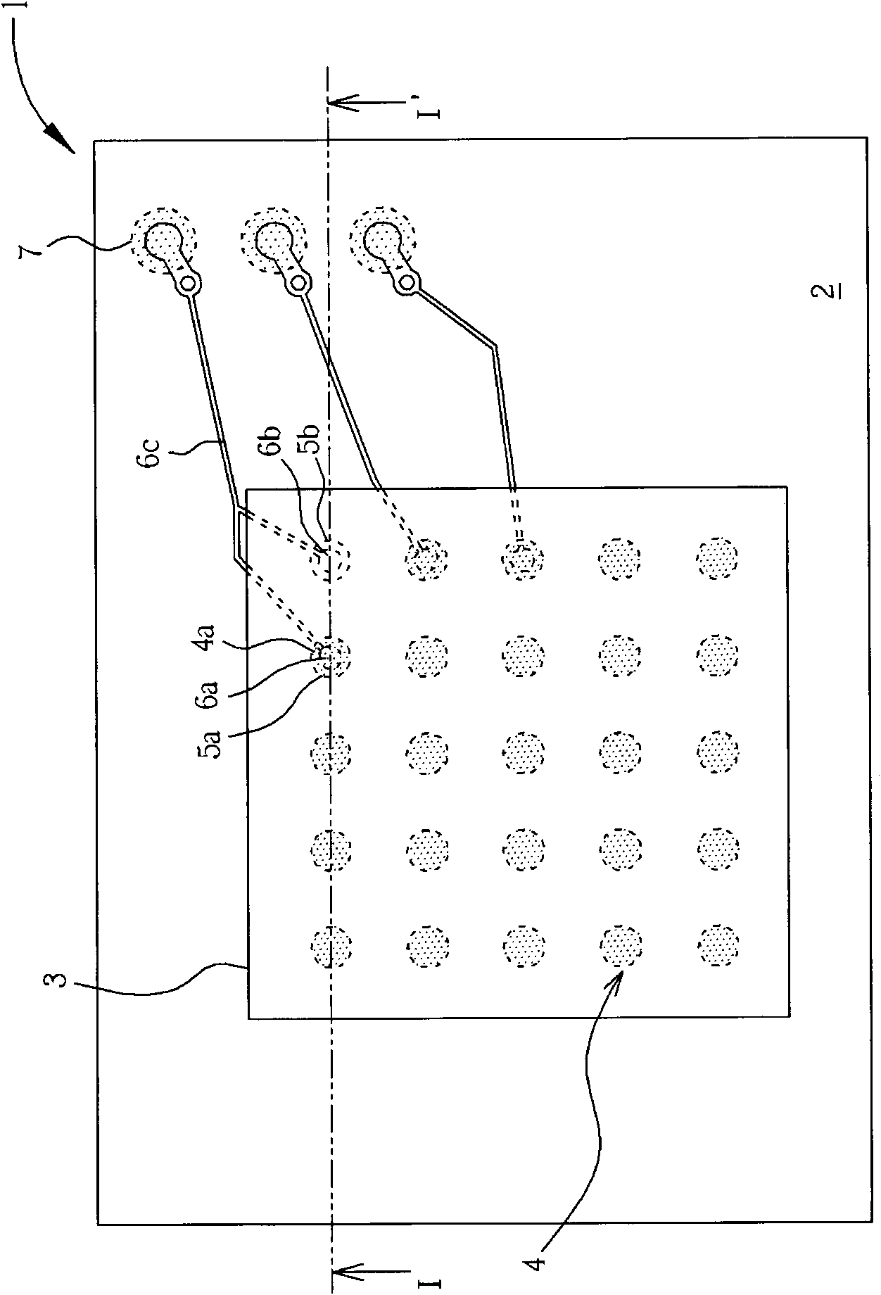
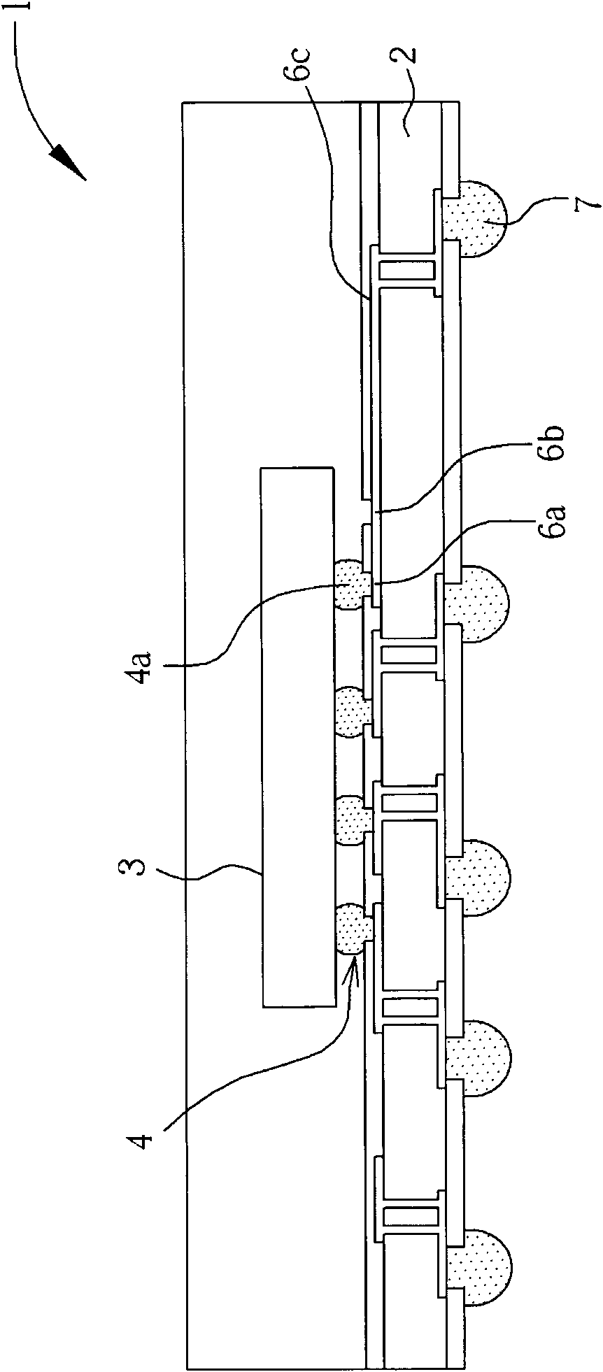
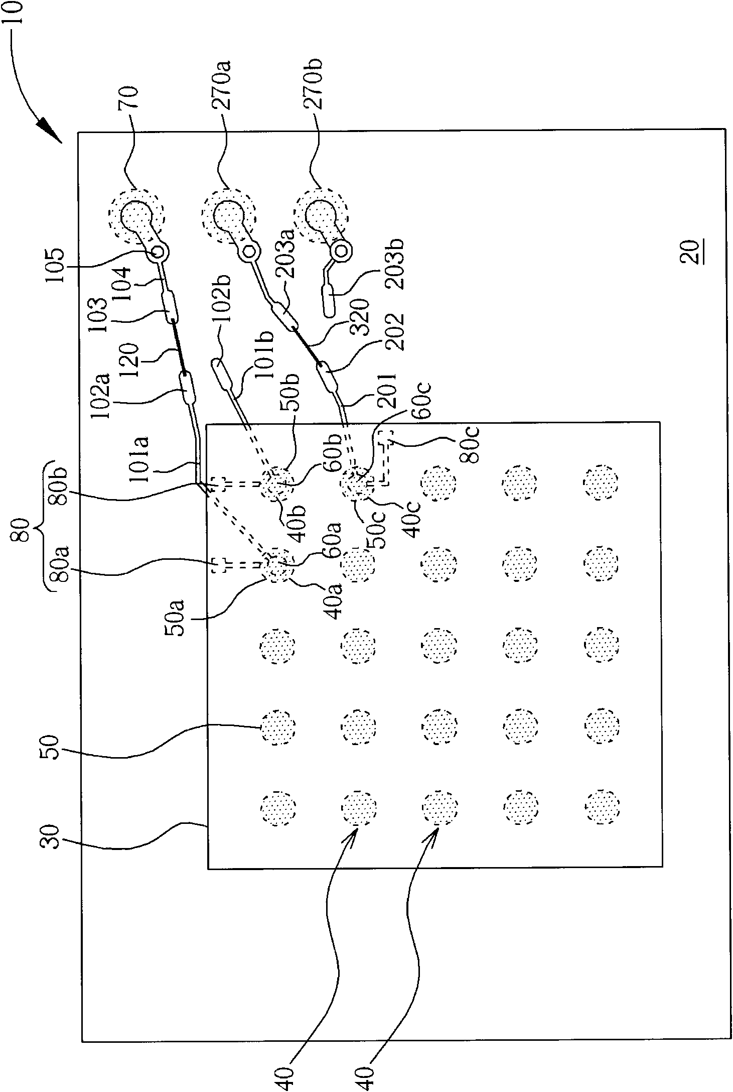
[0015] In order to make the purpose, features, and advantages of the present invention more comprehensible, preferred embodiments are specifically described below for detailed description. The examples are used to illustrate the present invention, not to limit the present invention. The protection scope of the present invention shall be determined by the appended claims.

[0016] Certain terms are used throughout the specification and following claims to refer to particular components. It should be understood by those skilled in the art that hardware manufacturers may refer to the same component by different terms. This description and the following claims do not use the difference in name as a way to distinguish components, but use the difference in function of components as a criterion for distinguishing. The "comprising" mentioned throughout the specification and subsequent claims is an open term, so it should be interpreted as "including but not limited to". Otherwise, ...


PUM


Abstract

This invention provides a semiconductor flip chip package including a carrier substrate and a flip chip electrically coupled to the carrier substrate by a plurality of interconnections. A first input / output (I / O) terminal of the semiconductor flip chip package and a bond wire electrically couple the first I / O terminal to a first interconnection of the plurality of interconnections at a first surface of the carrier substrate. The semiconductor flip chip package is more flexible and is lower in cost.

Description

technical field [0001] The present invention relates to semiconductor packaging, and more particularly to semiconductor flip-chip packaging. Background technique [0002] In general, flip-chip technology is widely used in various consumer products where the form factor is particularly important, such as mobile phones, camcorders (camcorders) or personal digital assistants (Personal Digital Assistant, PDA). The need for performance and the ability to use flip-chip designs to achieve smaller dies are driving the use of flip-chip packaging in many applications. Smaller die means a higher number of die per wafer. While flip-chip assembly has brought benefits to high-performance components, its cost has also become a major challenge for mainstream applications. Therefore, much effort needs to continue to be made to reduce costs. [0003] figure 1 A top view of a flip-chip package with specific bump options according to the prior art. figure 2 for along figure 1 Schematic d...

Claims


Application Information

Patent Timeline
Patent Type & Authority Applications(China)
IPC IPC(8): H01L23/485
CPCH01L2924/19107H01L23/5382H01L2224/16225H01L23/49816H01L2924/15311H01L23/49827
Inventor 谢东宪
Owner MEDIATEK INC
Why Eureka
Try Eureka