Light emitting semiconductor device, light emitting semiconductor module and lighting device

A light-emitting device and light-emitting module technology, applied in the direction of lighting devices, lighting device parts, semiconductor devices, etc., can solve the problems of lack of light dispersion, inappropriate street lighting, and inability to make crime-preventing street lights, etc., to improve convergence sexual effect

Inactive Publication Date: 2011-04-27
SANKEN ELECTRIC CO LTD
View PDF4 Cites 2 Cited by
  • Summary
  • Abstract
  • Description
  • Claims
  • Application Information

AI Technical Summary

Problems solved by technology

However, even in a semiconductor light-emitting device equipped with this lens, since dispersion of light in the width direction of the package substrate is hardly obtained, and because the illumination around street lamps is not suitable, measures for crime prevention cannot be made. suitable street light

Method used


Image

  • Light emitting semiconductor device, light emitting semiconductor module and lighting device
  • Light emitting semiconductor device, light emitting semiconductor module and lighting device
  • Light emitting semiconductor device, light emitting semiconductor module and lighting device

Examples


Embodiment 1

[0064] Embodiment 1 of the present invention describes a semiconductor light-emitting device as a light-emitting source of a street lamp, a semiconductor light-emitting module incorporating the semiconductor light-emitting device, and a system equipped with the semiconductor light-emitting module, which are used in lighting devices, especially road or sidewalk illumination. An example of the present invention is applied to a lighting device.

[0065] [Overall structure of semiconductor light emitting device]

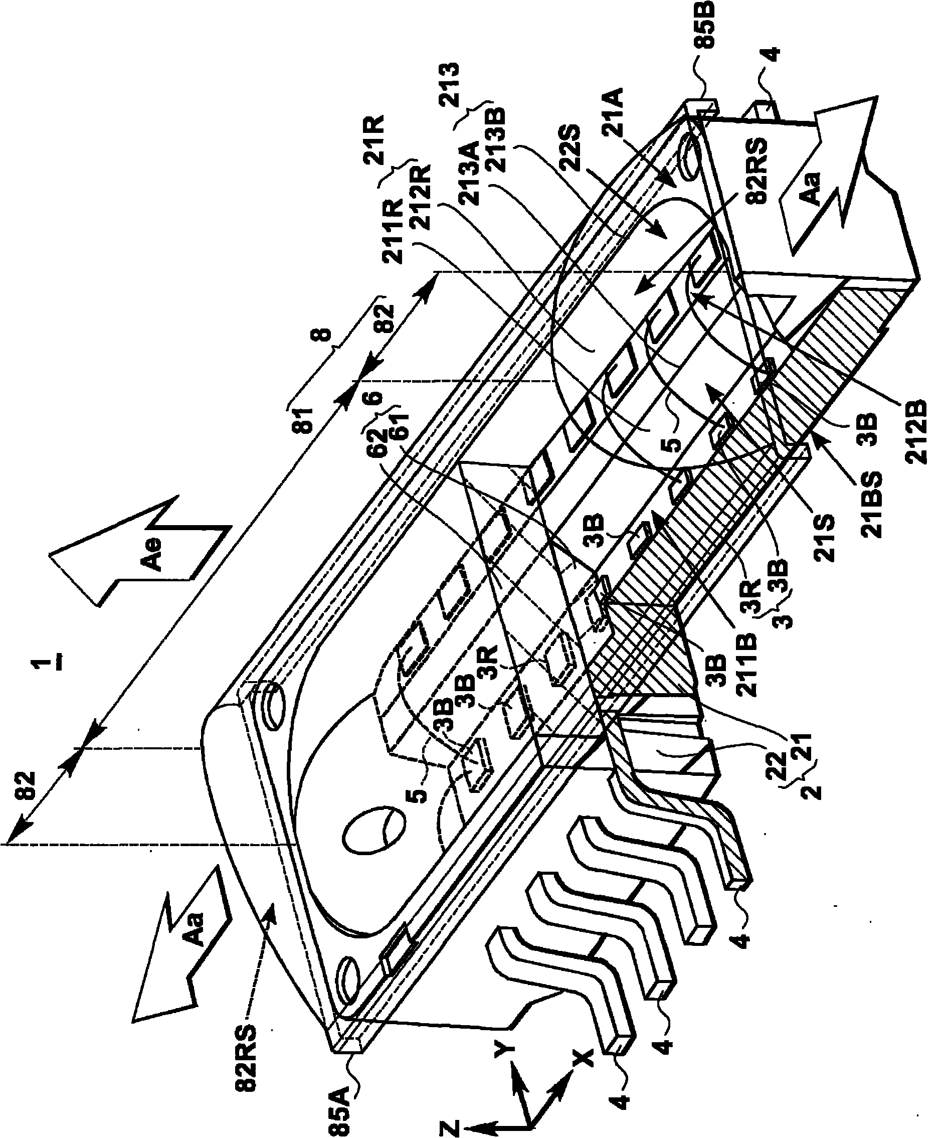
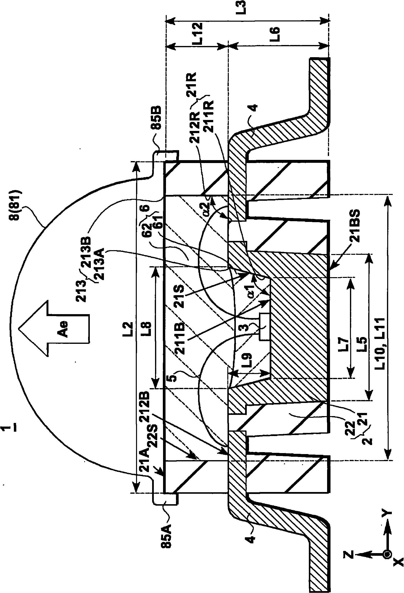
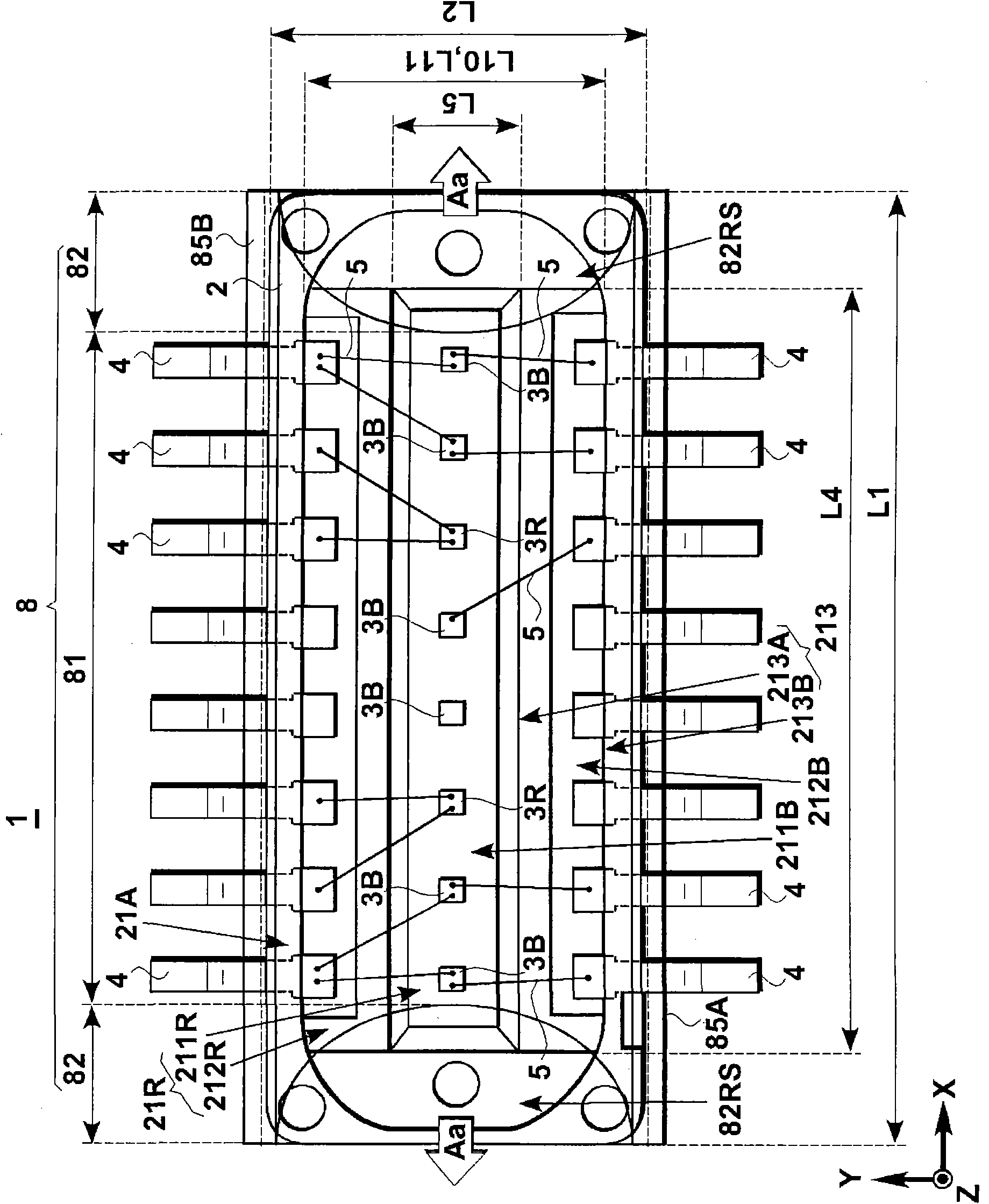
[0066] Such as Figure 1 to Figure 3 As shown, the semiconductor light-emitting device 1 of Embodiment 1 has: a package substrate 2 having a groove 21R, and the groove 21R constitutes an opening whose dimension in the first direction X is longer than the dimension in the second direction Y intersecting the first direction X. 213; a plurality of light emitting elements 3 arranged in the first direction X at the bottom 211B of the groove 21R; a light-transmitting resin 6 ...

Embodiment 2

[0133] Embodiment 2 of the present invention is for describing a modified example of condenser lens 8 of semiconductor light emitting device 1 in Embodiment 1 described above.

[0134] [Structure of semiconductor light emitting device and condenser lens]

[0135] Such as Figure 17 As shown, in the semiconductor light emitting device 1 of the second embodiment, the refraction surface 82RS of the sub-lens region 82 of the condenser lens 8 is at the opening 213 of the groove 21R of the package substrate 2, more specifically, at the second opening of the second groove 212R. One end and the other end of the opening 213B in the first direction X are disposed outside the second opening 213B in the first direction X. That is, the refractive surface 82RS of the sub-lens region 82 is not arranged at a position overlapping the second opening 213B in plan view (viewed from the light emission direction Ae or the third direction Z), but is arranged outside the second opening 213B. In the...

Embodiment 3

[0141] Embodiment 3 of the present invention is for describing a modified example of condenser lens 8 of semiconductor light emitting device 1 of Embodiment 2 described above.

[0142] [Structure of semiconductor light emitting device and condenser lens]

[0143] Such as Figure 18 to Figure 20 As shown, in the semiconductor light emitting device 1 of the third embodiment, the refraction surface 82RS of the sub-lens region 82 of the condenser lens 8 is at the opening 213 of the groove 21R of the package substrate 2, more specifically, at the second opening of the second groove 212R. One end and the other end of the opening 213B in the first direction X are arranged on the outside of the second opening 213B in the first direction X, and are configured to oppose light emitted from the light emitting element 3 in the first direction X (light dispersion direction Aa). The condensing surface on which the light passing through the second opening 213B is condensed.

[0144] Similar...


PUM


Abstract

The invention provides a light emitting semiconductor device, a light emitting semiconductor module and a lighting device. The light emitting semiconductor device (1) is provided with: a packaged substrate (2) provided with a groove (21R) forming an opening having the size of a first direction (X) longer than the size of a second direction (Y); light emitting elements (3) are many and disposed in the first direction (X) of the bottom (211B) of the groove (21R); light transmission resin (6) is disposed in the groove (21R) to cover the light emitting elements (3); and a collector lens (8) converging light emitted from the light-emitting elements (3) and through an opening to a light outgoing direction (Ae) of the second direction (Y), a main lens zone (81) keeping converged proportion at a certain proportion in the first direction (X), and secondary lens zones (82) at one end and the other end of the first direction (X) making light emitted by the light-emitting elements (3) perform refraction toward the first direction (X).

Description

technical field [0001] The present invention relates to a semiconductor light emitting device, a semiconductor light emitting module and a lighting device, in particular to a semiconductor light emitting device suitable for lighting, a modularized semiconductor light emitting module of the semiconductor light emitting device and a lighting device incorporating the semiconductor light emitting module. Background technique [0002] There is a tendency to use a semiconductor light emitting device as a light emitting source of a backlight of a liquid crystal display (LCD: liquid crystal display). The semiconductor light emitting device is specifically a light emitting diode (LED: light emitting diodes). A light-emitting diode is a light-emitting source that consumes little power, has a long life, and is suitable for an environment that does not contain harmful substances such as mercury. [0003] The backlight includes a light guide plate arranged on the back surface of the liq...

Claims


Application Information

Patent Timeline
Patent Type & Authority Applications(China)
IPC IPC(8): H01L33/48H01L33/58G02B6/42F21S2/00F21V5/04F21Y101/02
CPCH01L2224/48247H01L2224/45144H01L2224/48091H01L2924/00014H01L2924/00
Inventor 大塚康二
Owner SANKEN ELECTRIC CO LTD
Why Eureka
Try Eureka