Supercharge Your Innovation With Domain-Expert AI Agents!

Photonic crystal microcavity laser

A technology of photonic crystal microcavity and photonic crystal, applied in the structure of optical resonant cavity, structure of optical waveguide semiconductor, etc., can solve the problems of increased number of cavity modes, low Q value, large volume, etc., and achieve less number of microcavity modes , Improve the enhancement effect, the effect of large microcavity volume

Active Publication Date: 2012-06-27
INST OF SEMICONDUCTORS - CHINESE ACAD OF SCI
View PDF0 Cites 0 Cited by
  • Summary
  • Abstract
  • Description
  • Claims
  • Application Information

AI Technical Summary

Problems solved by technology

However, due to the large volume of the regular hexagonal Hn (n>2) cavity, the number of cavity modes increases significantly, and the Q value is low. A series of resonance peaks will appear in the entire spectral line, and it is difficult to achieve single-mode conditions. Theoretically, its Luminescence enhancement is not as effective as single-point defect cavities with smaller microcavities

Method used


Image

  • Photonic crystal microcavity laser
  • Photonic crystal microcavity laser
  • Photonic crystal microcavity laser

Examples


Embodiment Construction

[0026] In order to make the object, technical solution and advantages of the present invention clearer, the present invention will be described in further detail below in conjunction with specific embodiments and with reference to the accompanying drawings.

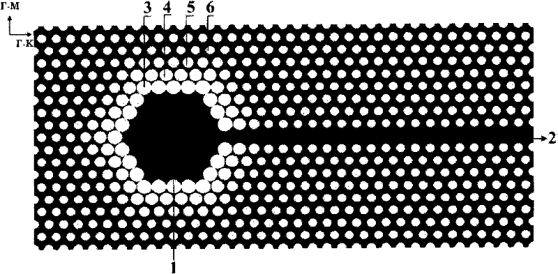
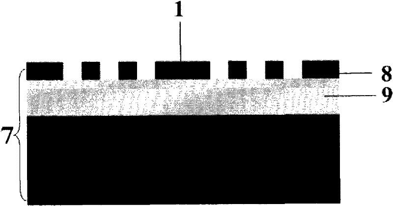
[0027] See attached figure 1 and 2 , the photonic crystal microcavity 1 of the photonic crystal microcavity laser in this embodiment is a complete two-dimensional flat triangular lattice air-hole photonic crystal on the top layer of silicon 8 of the SOI substrate 7, and removes the edges formed by several air holes in the middle A regular hexagonal H4 microcavity with a length of 4 lattice constants is implanted with erbium ions and oxygen ions into the photonic crystal microcavity 1, and an active region is formed after high temperature annealing. Starting from one end point of the hexagon of the photonic crystal microcavity 1, a row of air holes are removed along the direction of the photonic crystal Γ-K to form the ou...


PUM


Abstract

The invention discloses a photonic crystal microcavity laser which comprises a photonic crystal microcavity and an output waveguide, wherein the photonic crystal microcavity is formed by removing a plurality of air holes from a complete two-dimensional panel triangular lattice air hole type photonic crystal on an SOI (Silicon On Insulator) and is a regular hexagonal H4 type microcavity of which the side length is four lattice constants; three layers of air holes near to the photonic crystal microcavity are respectively first nearest air holes, second nearest air holes and third nearest air holes from inside to outside; rare earth ions and non-metal ions are injected into the photonic crystal microcavity to form an active region; and the output waveguide is a mongline fault formed by removing a row of air holes from an end point of the photonic crystal microcavity along a gamma-K direction of the photonic crystal. The structure of the laser has a larger microcavity volume and can improve the Q value of the microcavity, reduce the mode quantity of the microcavity and improve the enhancement effect of the microcavity on the lighting of an active medium.

Description

technical field [0001] The invention relates to the technical field of semiconductor light emitting devices, in particular to a photonic crystal microcavity laser. Background technique [0002] The photonic crystal-based microcavity structure can achieve high quality factor (Q value) and high radiation enhancement factor, and can achieve higher energy conversion efficiency. Due to the limitation of semiconductor processing technology, the current research is more on the two-dimensional planar photonic crystal microcavity structure with limited thickness in the vertical direction. There are two types of Ln (n represents the number of air holes removed from the microcavity). Among them, H1 and L3 are the two simplest types of microcavities that have been studied more. By changing the structural parameters of the air holes near the microcavities or moving their positions, microcavities with extremely high Q values ​​can be obtained. However, these two types of microcavities a...

Claims


Application Information

Patent Timeline
Patent Type & Authority Patents(China)
IPC IPC(8): H01S5/20H01S5/10
Inventor 张家顺王玥吴远大安俊明王红杰李建光胡雄伟
Owner INST OF SEMICONDUCTORS - CHINESE ACAD OF SCI
Features
  • R&D
  • Intellectual Property
  • Life Sciences
  • Materials
  • Tech Scout
  • Unparalleled Data Quality
  • Higher Quality Content
  • 60% Fewer Hallucinations
Learn More