Circuit board structure

A technology for circuit boards and circuit daughter boards, which is applied in the structural connection of printed circuits, printed circuits, and multi-layer circuit manufacturing, etc.

Active Publication Date: 2011-05-04
UNIMICRON TECH CORP
View PDF0 Cites 9 Cited by
  • Summary
  • Abstract
  • Description
  • Claims
  • Application Information

AI Technical Summary

Problems solved by technology

It is worth noting that in a circuit board with local high wiring density, the area of ​​high wiring density only accounts for a part of the entire circuit board, and the rest of the area is the general layout (low wiring density) lines, but due to the lack of innovation in the process, now The known production method still needs a long time, so the production cost has not been reduced, and it is not economical
[0005] This shows that the above-mentioned existing printed circuit board obviously still has inconvenience and defects in structure and use, and needs to be further improved urgently.
In order to solve the above-mentioned problems, the relevant manufacturers have tried their best to find a solution, but no suitable design has been developed for a long time, and the general products do not have a suitable structure to solve the above-mentioned problems. This is obviously related. The problem that the industry is eager to solve

Method used


Image

  • Circuit board structure
  • Circuit board structure
  • Circuit board structure

Examples


Embodiment Construction

[0030] In order to further explain the technical means and effects of the present invention to achieve the intended purpose of the invention, below in conjunction with the accompanying drawings and preferred embodiments, the specific implementation, structure, features and effects of the circuit board structure proposed according to the present invention, Details are as follows.

[0031] The aforementioned and other technical contents, features and effects of the present invention will be clearly presented in the following detailed description of preferred embodiments with reference to the drawings. Through the description of the specific implementation, it should be possible to obtain a deeper and more specific understanding of the technical means and effects of the present invention to achieve the intended purpose, but the attached drawings are only for reference and description, not for the purpose of the present invention. be restricted.

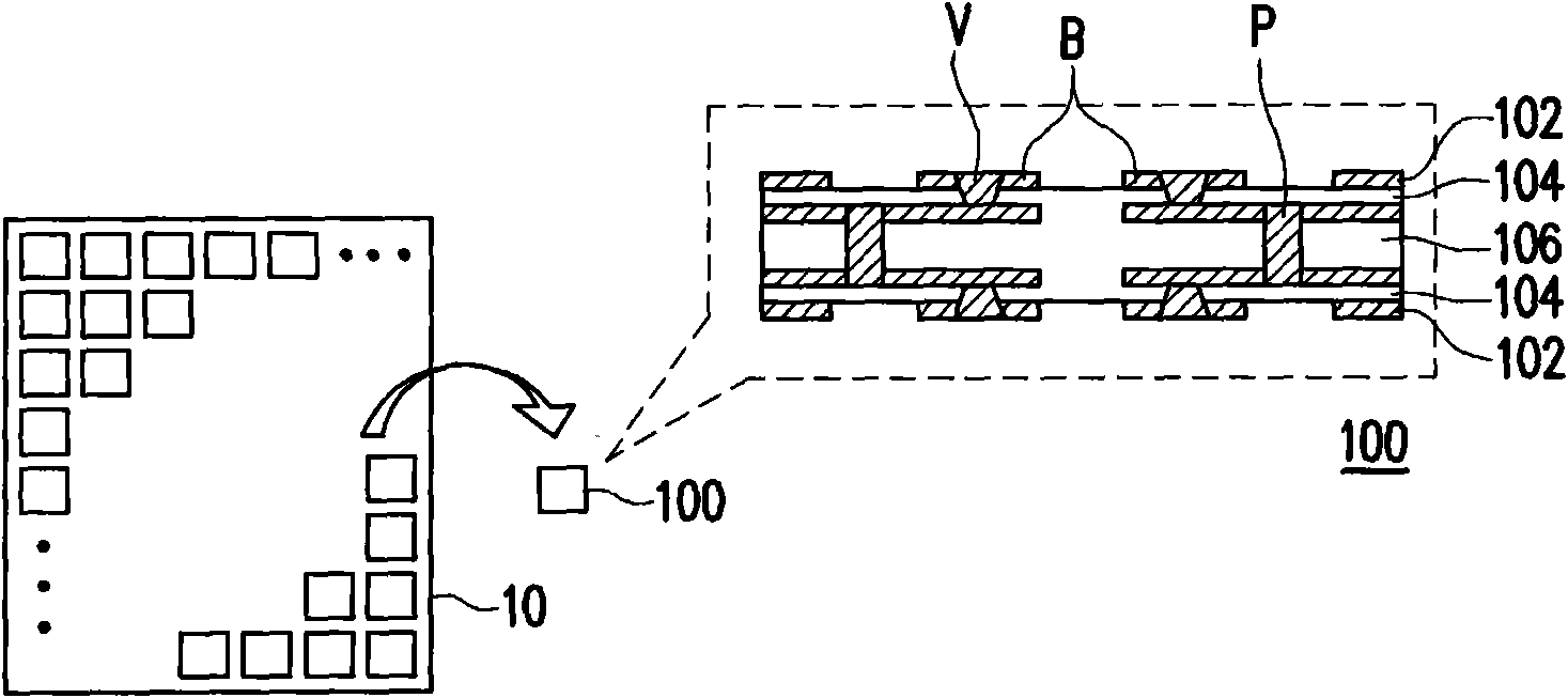
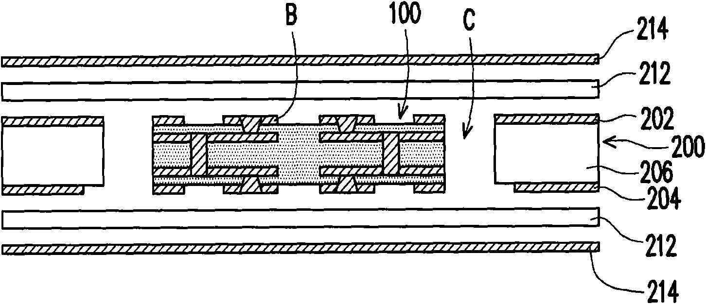
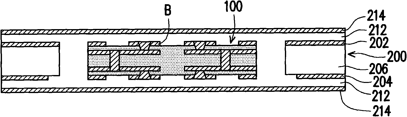
[0032] Figure 1A ~ Figure 1E Ea...


PUM


Abstract

The invention relates to a circuit board structure, which comprises an inner circuit board and a circuit sub board, wherein the inner circuit board is provided with a first circuit layer, a second circuit layer and a core layer positioned between the first circuit layer and the second circuit layer; the circuit sub board is embedded in the core layer, and the wiring density of the circuit sub board is more than that of the inner circuit board. In addition, in another circuit board structure, at least one side of the circuit sub board correspondingly exposes in an opening region. Therefore, the invention is used for making the circuit board with high local wiring density, and can simplify the step and reduce the making cost.

Description

technical field [0001] The invention relates to a circuit board, in particular to a circuit board structure integrating high / low wiring density. Background technique [0002] The market demand for consumer electronic products is huge. In addition to powerful functions, consumers also require light, thin, short and small. It develops towards multi-layers, from two layers and four layers to six layers, eight layers, and even more than ten layers, so that electronic components can be more densely installed on printed circuit boards, reducing the area of ​​printed circuit boards, and making Electronics are smaller. [0003] However, as the number of layers of the printed circuit board increases, the manufacturing steps become extremely complicated, making the manufacturing time very long. In order to make circuits with high wiring density, the number of layers of printed circuit boards often exceeds four layers. , it will take about several hours, and if the subsequent proces...

Claims


Application Information

Patent Timeline
IPC IPC(8): H05K1/00H05K1/14H05K3/46
Inventor 张钦崇张振铨张宏麟黄瀚霈
Owner UNIMICRON TECH CORP
Why Eureka
Try Eureka