Method for measuring thickness of edge film of silicon wafer

An edge film, thickness measurement technology, applied in the direction of electric/magnetic thickness measurement, measurement device, electromagnetic measurement device, etc., can solve the problem of inaccurate edge film thickness value

Active Publication Date: 2011-05-11
HWATSING TECH
View PDF3 Cites 20 Cited by
  • Summary
  • Abstract
  • Description
  • Claims
  • Application Information

AI Technical Summary

Problems solved by technology

[0004] In order to solve the inaccurate problem of the edge film thickness value caused by the signal distortion existing when the existing eddy current sensor measures the edge film thickness, the present invention provides a method for measuring the edge

Method used


Image

  • Method for measuring thickness of edge film of silicon wafer
  • Method for measuring thickness of edge film of silicon wafer
  • Method for measuring thickness of edge film of silicon wafer

Examples


Embodiment Construction

[0032] Specific embodiments of the present invention will be described below in conjunction with the accompanying drawings.

[0033] The principle of the above solution is to use a mathematical algorithm to obtain an accurate silicon wafer edge film thickness without changing the film thickness measurement hardware.

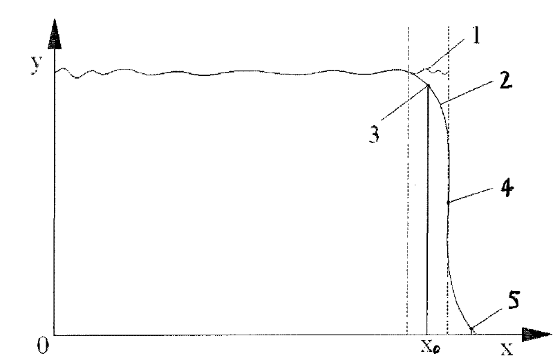
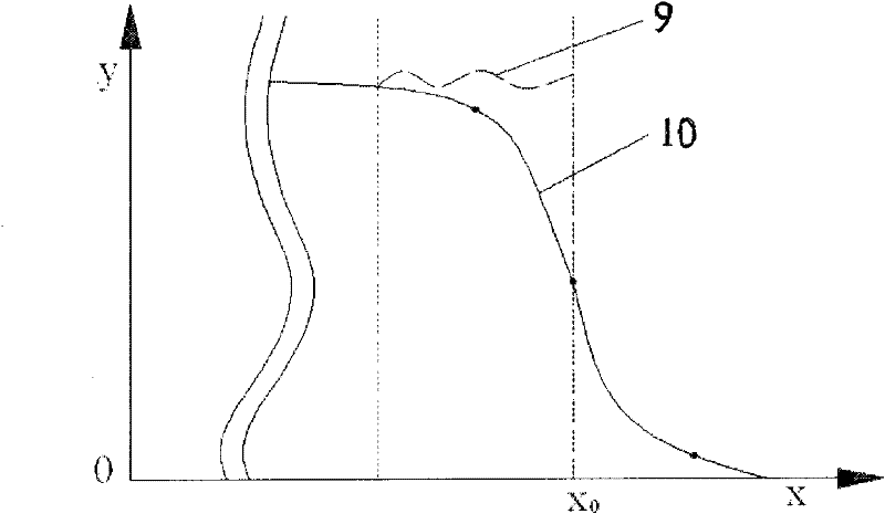
[0034] The mathematical model of the present invention is or x is the measured point, its range is x 0 -2D~x 0 Between, D is the diameter of the eddy current sensor, T m is the measured value of film thickness at point x, T r is the actual thickness value of film thickness at point x, x 0 film thickness edge point, d is the correction coefficient related to sensor size, shape, working distance, etc., t is the integral variable in The value between, film thickness measurement value T m It can be measured by the eddy current sensor, and the d obtained after calibration and the measured T m And the coordinates of point x are substituted into the model to ...


PUM


Abstract

A method for measuring the thickness of an edge film of a silicon wafer belongs to the technical field of thickness measurement of chemical mechanical polishing films. By use of a mathematical model provided in the invention, a measured curve of edge film thickness is corrected to be consistent with the actual curve of edge film thickness to the greatest extent, so that the measured value of edge film thickness can be used as the actual value of edge film thickness. The invention solves the problem of the prior art that the measured value of edge film thickness is distorted when the film thickness of the silicon wafer is measured by use of electric vortex, and has the advantages that only the mathematical model is needed to be corrected instead of the hardware equipment. When in use, only the simple off-line calibration is required, so as to avoid the influence on the yield of the chemical mechanical polishing process.

Description

technical field [0001] The invention relates to the technical field of chemical mechanical polishing film thickness measurement, in particular to a method for measuring the film thickness at the edge of a silicon wafer. Background technique [0002] Now that the wafer size has increased to 300mm, and will increase to 450mm in the near future, chips at the edge of the wafer have an increasing impact on the overall yield. Therefore, film thickness measurement at the edge of the silicon wafer during chemical mechanical polishing has become particularly important. [0003] Most of the copper film thickness and surface topography are measured by eddy current sensors before and after the chemical mechanical polishing process. The radius of the eddy current sensor probe is generally at least 6 ~ 8mm, such as figure 1 , figure 2 As shown, 6 and 7 are eddy-current sensors installed in pairs, and 8 is a silicon chip. During the measurement process, the silicon chip is figure 2 T...

Claims


Application Information

Patent Timeline
IPC IPC(8): B24B49/04B24B49/10
CPCB24B37/013B24B49/105G01B7/105G01B7/06G06F17/10
Inventor 路新春沈攀何永勇
Owner HWATSING TECH
Why Eureka
Try Eureka