Optical fiber array fixing device and manufacturing method thereof

A technology for fixing devices and optical fiber arrays, which is applied in optical components, instruments, optics, etc., can solve the problems of unfavorable large-scale optical switches, high cost of precision mold opening, and increased system cost, achieving strong scalability, reducing difficulty and Cost, effect of a wide range of functions

Inactive Publication Date: 2011-05-18
PEKING UNIV
View PDF4 Cites 1 Cited by
  • Summary
  • Abstract
  • Description
  • Claims
  • Application Information

AI Technical Summary

Problems solved by technology

However, there are huge difficulties in manufacturing high-precision, low-cost fiber array fixtures suitable for micro-optical devices such as medium and large-scale 2D optical switches and large-scale 3D optical switches.
As far as the current situation is concerned, the positioning of optical fiber grooves is still achieved by V-groove or precision mold opening in the world. For the former, although it has the advantage of low cost, it is not conducive to expanding to large-scale optical switches; for the latter, Although it can be applied to a wide range of optical switches, the cost of precision mold opening is very high, which will greatly increase the system cost

Method used


Image

  • Optical fiber array fixing device and manufacturing method thereof
  • Optical fiber array fixing device and manufacturing method thereof
  • Optical fiber array fixing device and manufacturing method thereof

Examples


Embodiment Construction

[0023] The optical fiber array fixing device and the preparation method thereof proposed by the present invention are described in detail as follows with reference to the accompanying drawings and embodiments.

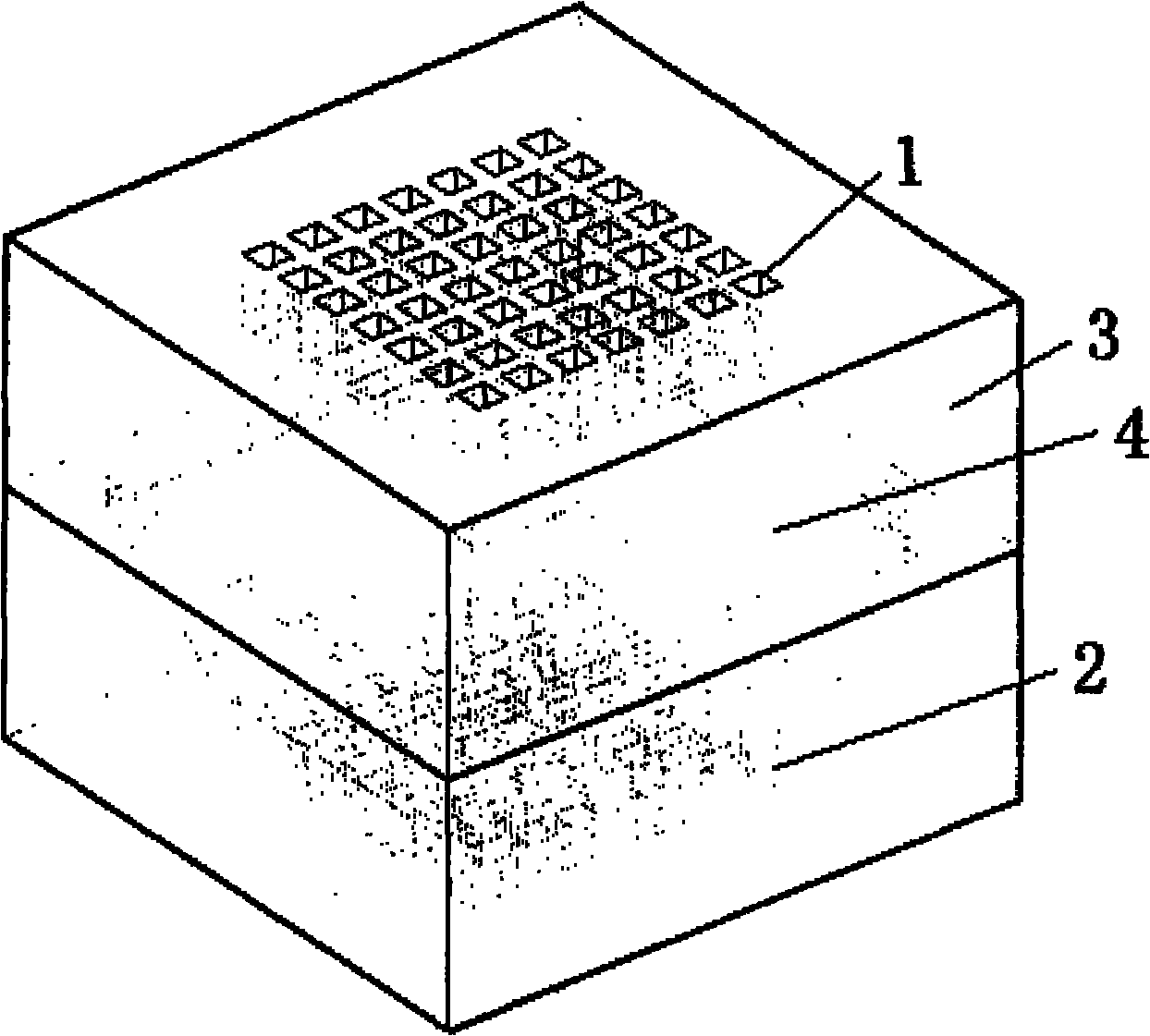
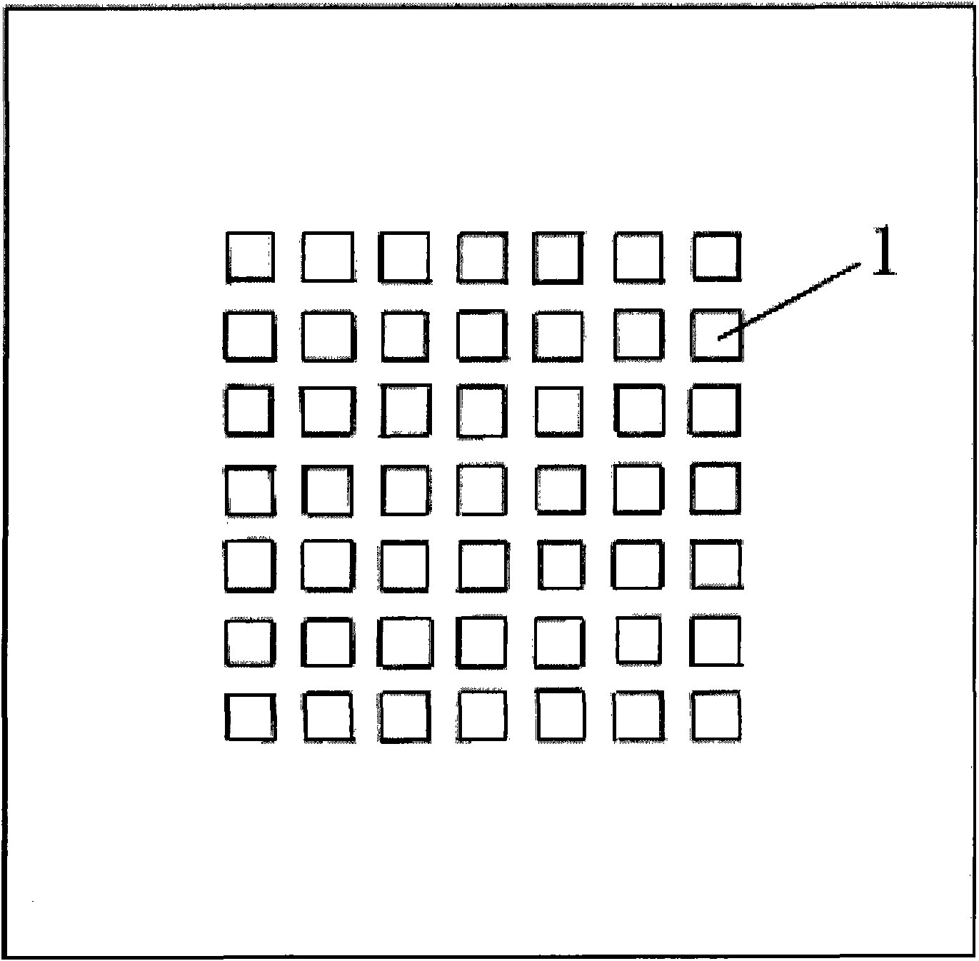
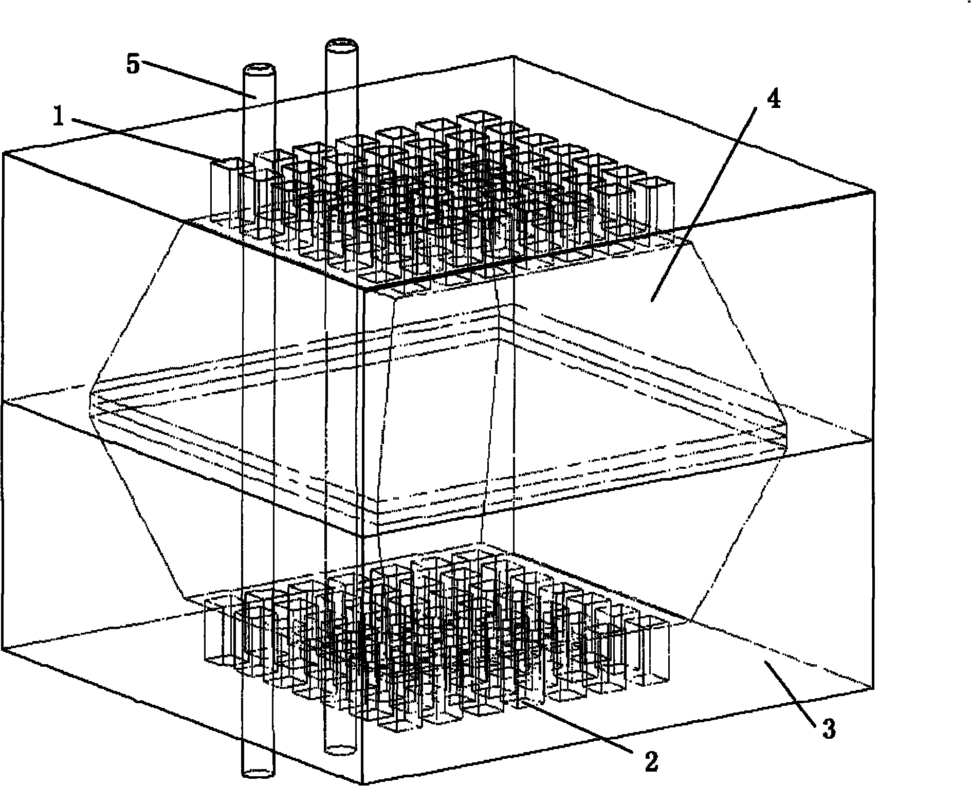
[0024] The optical fiber array fixing device of the invention is suitable for micro-optical devices such as medium and large-scale 2D optical switches and large-scale 3D optical switches. like figure 1 Shown is a perspective perspective view of an optical fiber array fixing device according to an embodiment of the present invention, the device includes: a base 3, and an optical fiber fixing hole array composed of several identical optical fiber fixing holes, and the optical fiber fixing holes are respectively arranged on the base. The upper and lower end faces of the base 3, and the optical fiber fixing holes 1 arranged on the upper end face and the optical fiber fixing holes 2 arranged on the lower end face correspond one-to-one. In order to achieve stable fixing, the...


PUM


Abstract

The invention relates to an optical fiber array fixing device and a manufacturing method thereof. The optical fiber array fixing device comprises a base, and an optical fiber fixing hole array which consists of a plurality of the same optical fiber fixing holes, wherein the optical fiber fixing hole array is arranged on upper and lower end faces of the base; the optical fiber fixing holes of the upper and lower end faces are in one-to-one correspondence; and a cavity is formed between the optical fiber fixing holes of the upper and lower end faces. The optical fiber array fixing device is suitable for medium-scale and large-scale two-dimensional (2D) optical switches, large-scale three-dimensional (3D) optical switches and the like, and has high expandability; optical fibers can be accurately and stably positioned by the optical fiber fixing holes defined by high-precision photolithography, so that the difficulty and cost of encapsulation are reduced. In the manufacturing method, the conventional micro-electromechanical system (MEMS) process equipment can be adopted, large-scale manufacturing is realized, the process is simple, and the manufacturing method is compatible with various types of MEMS device processes and can be used for realizing a micro-optical integrated system with wider and stronger functions.

Description

technical field [0001] The invention relates to the technical field of micro-electromechanical systems (Micro Electro Mechanical systems, MEMS) optical switches, in particular to an optical fiber array fixing device and a preparation method thereof. Background technique [0002] The optical switch realized by MEMS technology has the advantages of small size, light weight, low energy consumption and stable performance. With the rapid development of optical fiber communication technology and dense wavelength division multiplexing systems, MEMS optical switches, as important optical waveguide devices, have been more and more widely used. At present, there have been many reports on the research of MEMS optical switches. [0003] Fiber array fixed devices suitable for medium and large-scale 2D optical switches and large-scale 3D optical switches and other micro-optical devices are a key technology that needs to be broken through in the current development of MEMS optical switch ...

Claims


Application Information

Patent Timeline
Patent Type & Authority Applications(China)
IPC IPC(8): G02B6/12G02B6/136
Inventor 吴文刚
Owner PEKING UNIV
Why Eureka
Try Eureka