I2C (inter-integrated circuit) bus detection device

A detection device and bus technology, applied in error detection/correction, instruments, electrical digital data processing, etc., can solve the problems of complex circuit structure and high cost, and achieve the effect of simple circuit structure and low cost

Inactive Publication Date: 2011-05-18
HONG FU JIN PRECISION IND (SHENZHEN) CO LTD +1
3 Cites 8 Cited by

AI-Extracted Technical Summary

Problems solved by technology

[0003] However, in the design or use of the I2C bus, I2C bus detection equipment is often used to detect the data signals and clock signals on the bus, so as to debug and debug electronic equipment according to the clock and data signals on the I2C bus. ...

Method used

The I2C bus detection device of the present invention receives the clock signal and the data signal output by the I2C bus to be tested by the first and second triggers 41, 42, and outputs the corresponding trigger signal according to the clock signal and the data signal Give the microcontroller 44, so that the microcontroller 44 enables corresponding interrupts and captures clock signals and data signals on the I2C bus, and stores the clock signals and data signals in th...

Abstract

The invention provides an I2C (inter-integrated circuit) bus detection device. The device comprises a first trigger, an inverter, a second trigger, a microcontroller, a memory and a display interface, wherein a clear pin of the first trigger receives the clock signals output by clock lines of an I2C bus; a clock pin of the first trigger receives the data signals output by data lines of the I2C bus and outputs the first trigger signals; the input terminal of the inverter receives the data signals output by the data lines of the I2C bus and inverts the data signals; a clear pin of the second trigger receives the clock signals of the I2C bus; a clock pin of the second trigger is connected with the output terminal of the inverter to receive the inverted data signals and outputs the second trigger signals; a first interrupt pin of the microcontroller receives the first trigger signals, a second interrupt pin is connected with the second trigger signals and a third interrupt pin receives the clock signals of the I2C bus; an input pin of the microcontroller receives the data signals of the I2C bus; the memory is connected with an input/output pin of the microcontroller and is used for memorizing the data captured by the microcontroller; and the display interface is connected with an input/output pin of the microcontroller and is used for displaying the signals memorized in the memory.

Application Domain

Technology Topic

Image

  • I2C (inter-integrated circuit) bus detection device
  • I2C (inter-integrated circuit) bus detection device
  • I2C (inter-integrated circuit) bus detection device

Examples

  • Experimental program(1)

Example Embodiment

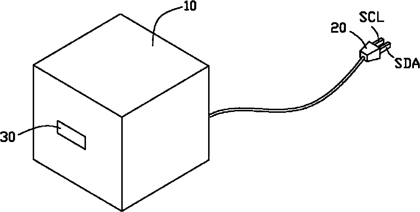
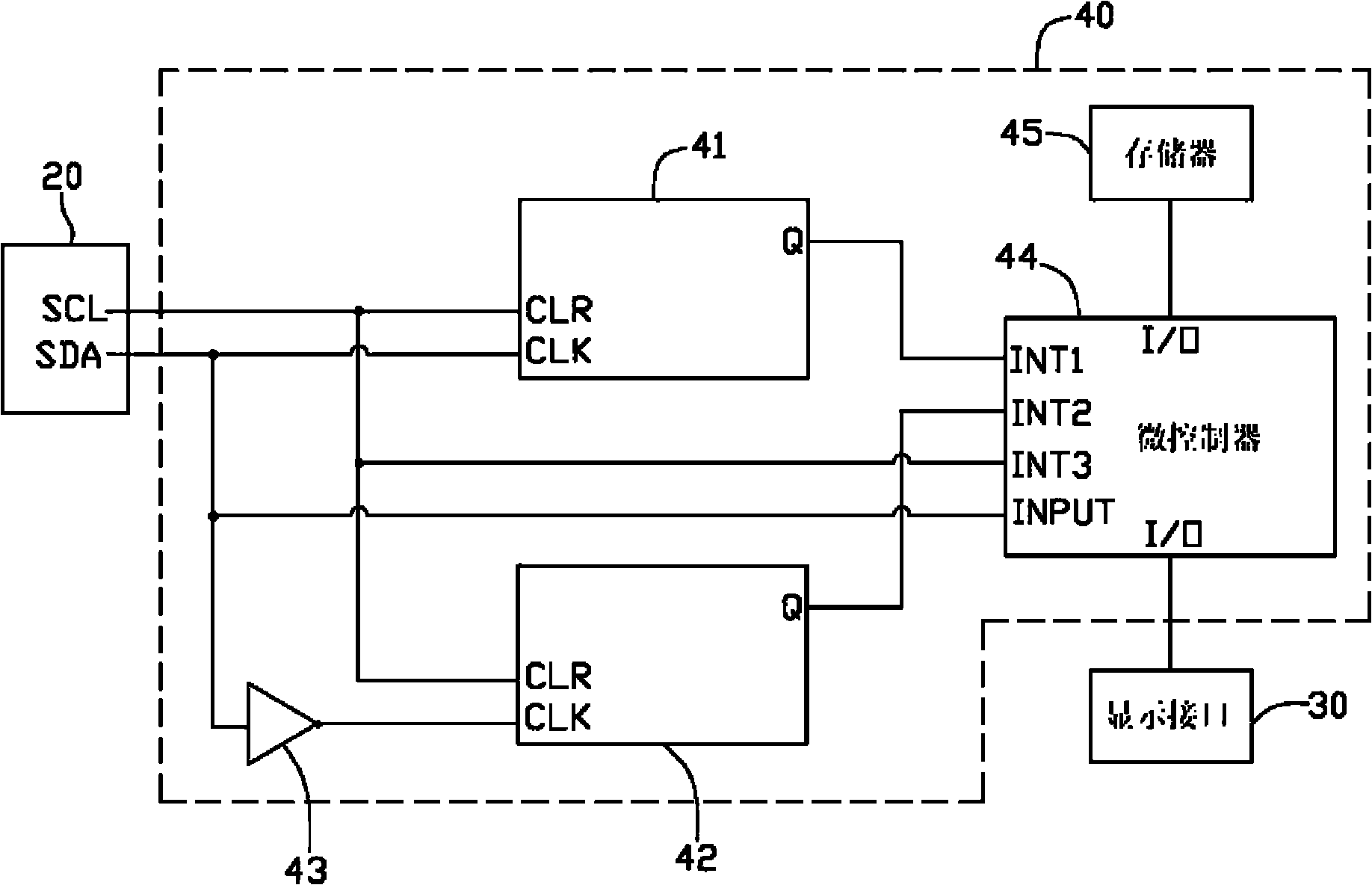
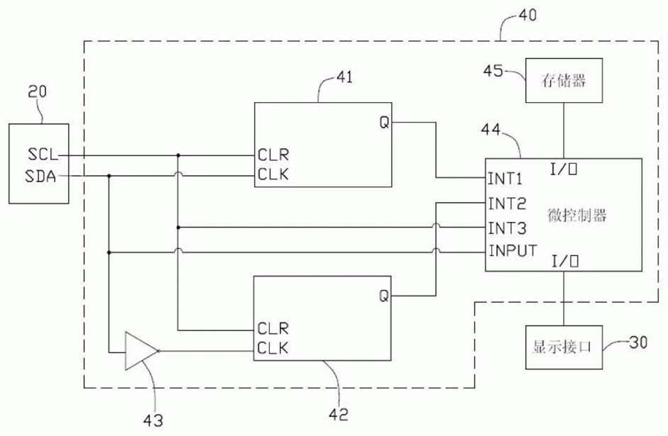
[0017] Please refer to figure 1 and figure 2 , the preferred embodiment of the I2C bus detection device of the present invention includes a casing 10, a connector 20 connected to the casing 10, a display interface 30 such as a VGA interface disposed on the casing 10, and a setting A detection circuit 40 inside the casing 10 and connected with the connector 20 and the display interface 30 . The connector 20 is used to connect the connector of the I2C bus to be detected on the main board of an electronic device, and the connector 20 includes a clock pin SCL and a data pin SDA, which are respectively used to connect the clock signal lines on the I2C bus. and a data signal line to receive the clock signal and data signal thereon, the display interface 30 is used to connect a display device to display the detection result processed by the detection circuit 40, so that the detection personnel can accurately Be aware of a problem with the motherboard of an electronic device.
[0018] In other embodiments, the housing 10 can also be a circuit board or other carrier that can be provided with circuits, and the connector 20 can also be other structures that can collect signals, such as a probe structure. The probe can be in contact with the clock signal line and the data signal line on the I2C bus. The display interface 30 can be other types of interfaces, and the above designs can be adjusted as required, and are not limited to this embodiment.
[0019] The detection circuit 40 includes two D flip-flops 41 and 42 , an inverter 43 , a microcontroller 44 and a memory 45 . The flip-flops 41 and 42 respectively receive the clock signal output by the clock pin SCL of the connector 20 and the data signal output by the data pin SDA, and output a trigger signal to the corresponding trigger signal according to the clock signal and the data signal. The microcontroller 44, so that the microcontroller 44 enables the corresponding interrupt and captures the clock signal and data signal on the I2C bus, and stores the clock signal and data signal in the memory 45 and through the The display interface 30 is displayed on the display device.
[0020] The clock pin SCL of the connector 20 is respectively connected to the clear pin CLR of the flip-flops 41 and 42 and the third interrupt pin INT3 of the microcontroller 44, and the data pin SDA of the connector 20 is respectively connected to the trigger pin INT3. The clock pin CLK of the controller 41, the input pin INPUT of the microcontroller 44 and the input end of the inverter 43, the output end of the inverter 43 is connected to the clock pin CLK of the flip-flop 42 , the output Q of the flip-flop 41 is connected to the first interrupt pin INT1 of the microcontroller 44, the output Q of the flip-flop 42 is connected to the second interrupt pin INT2 of the microcontroller 44, so The two input and output pins I/O of the microcontroller 44 are respectively connected to the memory 45 and the display interface 30 respectively.
[0021] During operation, the connector 20 is connected to the corresponding connector of the I2C bus to be collected, and the microcontroller 44 is connected to the display device through the display interface 30 . When the clock signal output by the clock pin SCL of the connector 20 is at a high level, and the data signal output by the data pin SDA of the connector 20 does not change, the flip-flops 41 and 42 do not work, so the The third interrupt pin INT3 of the microcontroller 44 receives the high-level signal and enables interruption, and the microcontroller 44 captures the data signal on the I2C bus through the input pin INPUT and stores it in the memory 45 and displayed on the display device through the display interface 30; when the data signal output by the data pin SDA of the connector 20 is at the falling edge, the clock pin of the flip-flop 41 CLK does not work after receiving the falling edge signal, the inverter 43 inverts the falling edge signal to a rising edge signal and supplies it to the clock pin CLK of the flip-flop 42 to make the flip-flop 42 work, so The second interrupt pin INT2 of the microcontroller 44 receives the rising edge signal output by the output end Q of the flip-flop 42 and enables interruption, and the microcontroller 44 captures the start state in the data signal on the I2C bus. The signal is stored in the memory 45 and displayed on the display device through the display interface 30; when the data signal output by the data pin SDA of the connector 20 is on a rising edge, the inversion The controller 43 inverts the rising edge signal to a falling edge signal and provides it to the clock pin CLK of the flip-flop 42, and the clock pin CLK of the flip-flop 42 does not work after receiving the falling edge signal, and the flip-flop 42 does not work. The clock pin CLK of 41 receives the rising edge signal to work, and the first interrupt pin INT1 of the microcontroller 44 receives the rising edge signal output by the output end Q of the flip-flop 41 to enable interrupting. The microcontroller 44 captures the stop state signal in the data signal on the I2C bus and stores it in the memory 45 and displays it on the display device through the display interface 30 . The tester can accurately know the problems existing on the main board of the electronic device according to the detection result displayed on the display device, so as to quickly and accurately complete the debugging or debugging of the electronic device.
[0022] The I2C bus detection device of the present invention receives the clock signal and data signal output by the I2C bus to be tested through the first and second flip-flops 41 and 42, and outputs a trigger signal to the Microcontroller 44, so that the microcontroller 44 enables the corresponding interrupt and captures the clock signal and data signal on the I2C bus, and stores the clock signal and data signal in the memory 43 and displays them in the same on the display device connected to the display interface 30 . The I2C bus detection device can automatically detect the I2C bus on the main board of the electronic equipment, and display the detection result to the tester through the display device, thereby avoiding the debugging caused by human negligence in the process of measuring the signal. or debug errors. The I2C bus detection device has a simple circuit structure and low cost.

PUM

no PUM

Description & Claims & Application Information

We can also present the details of the Description, Claims and Application information to help users get a comprehensive understanding of the technical details of the patent, such as background art, summary of invention, brief description of drawings, description of embodiments, and other original content. On the other hand, users can also determine the specific scope of protection of the technology through the list of claims; as well as understand the changes in the life cycle of the technology with the presentation of the patent timeline. Login to view more.

Similar technology patents

Classification and recommendation of technical efficacy words

  • Simple circuit structure
  • Low cost

Semiconductor device

InactiveUS6975142B2Low costReduce manufacturing stepsTransistorSolid-state devicesVoltage amplitudeSemiconductor
Owner:SEMICON ENERGY LAB CO LTD
Why Eureka
Try Eureka