Chip peeling device

A technology for stripping devices and chips, which is applied in the manufacture of electrical components, circuits, semiconductors/solid-state devices, etc. It can solve the problems of thimble height changes, wear, and inability to be picked up, and achieve the effect of ensuring repeatability

Inactive Publication Date: 2011-05-25
HUAZHONG UNIV OF SCI & TECH
View PDF4 Cites 28 Cited by
  • Summary
  • Abstract
  • Description
  • Claims
  • Application Information

AI Technical Summary

Problems solved by technology

[0003] However, there are the following problems in the method of separating the semiconductor chip from the blue film using the thimble: (1) the thimble is fragile and easy to break, and it is prone to wear and tear after long-term work, resulting in changes in the height of the thimble, resulting in insufficient peeling of the chip and cannot be removed. Picking, the general factory stipulates that the thimble needs to be replaced once a week to ensure the success rate of peeling if the thimble does not break. It is required to complete the replacement of the thimble within a few minutes, and the height and position must be consistent after each replacement of the thimble.
(2) When the chip is picked up, the center of the thimble, the center of the chip and the center of the chip pick-up device are the most favorable for chip peeling and pick-up. In some equipment, the center of the chip pick-up device is fixed. Due to processing and Due to the existence of assembly errors, it is impossible to ensure that the center of the thimble is aligned with the center of the pick-up device. Therefore, the chip peeling device needs to have a position adjustment function

Method used


Image

  • Chip peeling device
  • Chip peeling device
  • Chip peeling device

Examples


Embodiment Construction

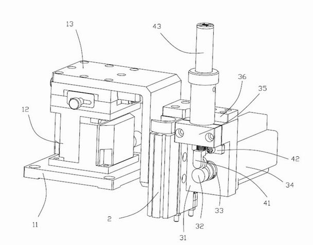
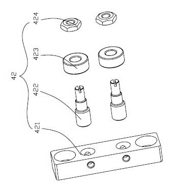
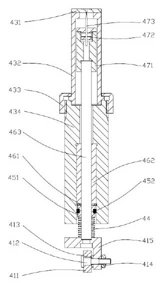
[0013] The chip peeling device of the present invention mainly includes thimble clamping and moving parts and a rotating drive part, and as an optimization, it also includes a lifting mechanism and a three-degree-of-freedom alignment platform. figure 1 It is a schematic diagram of the overall structure of a specific embodiment of the present invention, combined below Figure 1~3 Describe it in detail.

[0014] Such as figure 1 As shown, the supporting components of the device include a connection base plate 11 , a three-degree-of-freedom alignment platform 12 and an L-shaped plate 13 . The connecting bottom plate 11 is connected to the substrate by screws; the three-degree-of-freedom alignment platform 12 is the core part of the support component, which is composed of a Z-direction adjustment platform and an XY-direction adjustment platform, and the Z-direction adjustment platform is located below the XY-direction adjustment platform. The three-degree-of-freedom alignment pl...


PUM


Abstract

The invention provides a chip peeling device, which comprises a thimble clamping and moving assembly and a rotary driving assembly, wherein the thimble clamping and moving assembly comprises a thimble shaft supporting piece, a thimble shaft is fixed on the thimble shaft supporting piece, the exterior of the thimble shaft is provided with a thimble shaft sleeve, the top of the thimble shaft extends out of the thimble shaft sleeve and is connected with a thimble clamping piece, and the bottom of the thimble shaft is sleeved with a compression spring; and the exterior of the thimble clamping piece is provided with a thimble outer cover, and the top center of the thimble outer cover is provided with a pore through which a thimble extends out. As optimization, the chip peeling device also comprises a lifting mechanism and a three-degree-of-freedom alignment platform, wherein the lifting mechanism is used for realizing integral lifting of the thimble clamping and moving assembly and the rotary driving assembly; and the three-degree-of-freedom alignment platform is used for adjusting the position of the thimble in three directions X, Y and Z. The chip peeling device is very convenient to adjust the position of the center of the thimble, ensures that the center of the thimble is aligned with the center of a pickup device, is also very convenient to realize replacement of the thimble, and ensures the height and position consistency of the replaced thimble.

Description

technical field [0001] The invention relates to the field of electronic packaging, in particular to a device for peeling off a chip attached to a blue film from a wafer. Background technique [0002] Generally, the semiconductor wafer after the previous process is separated along the scribing line and the chip dividing line, and a plurality of semiconductor chips are formed by dicing. These semiconductor chips are pasted on an adhesive sheet (blue film) to form a wafer, and then the semiconductor chips are picked up one by one from the above blue film by a chip picker, and after the packaging process, the semiconductor chips form a semiconductor device. When picking up the semiconductor chip from the wafer, the following method is often used: the blue film pasted with the above-mentioned semiconductor chip is adsorbed and held by the upper surface of the chip peeling device, and the semiconductor chip is pushed up from below by the sharp thimble at the top of the chip peelin...

Claims


Application Information

Patent Timeline
Patent Type & Authority Applications(China)
IPC IPC(8): H01L21/00H01L21/68
Inventor 尹周平蔡伟林向邦懋王瑜辉熊有伦
Owner HUAZHONG UNIV OF SCI & TECH
Why Eureka
Try Eureka