Waveguide transfer device

A waveguide conversion and waveguide cavity technology, which is used in connection devices, waveguide-type devices, electrical components, etc., can solve the problems of high positioning accuracy, complex assembly, poor performance consistency, etc., so as to improve electrical performance consistency and reduce assembly. The effect of complexity

Inactive Publication Date: 2011-06-01
HUAWEI TECH CO LTD
View PDF5 Cites 5 Cited by
  • Summary
  • Abstract
  • Description
  • Claims
  • Application Information

AI Technical Summary

Problems solved by technology

[0005] After the waveguide conversion device is pasted on the multi-layer circuit board, the two-layer circuit board where the waveguide conversion device is located needs to be electrically connected to the transceiver system of the multi-layer circuit board, so the two-layer board is assembled on the For the multi-layer board, the positioning accuracy is relatively high, the assembly is relatively complicated, and the performance consistency is poor

Method used


Image

  • Waveguide transfer device
  • Waveguide transfer device
  • Waveguide transfer device

Examples


Embodiment Construction

[0021] The following will clearly and completely describe the technical solutions in the embodiments of the present invention with reference to the accompanying drawings in the embodiments of the present invention. Obviously, the described embodiments are only some, not all, embodiments of the present invention. Based on the embodiments of the present invention, all other embodiments obtained by persons of ordinary skill in the art without creative efforts fall within the protection scope of the present invention.

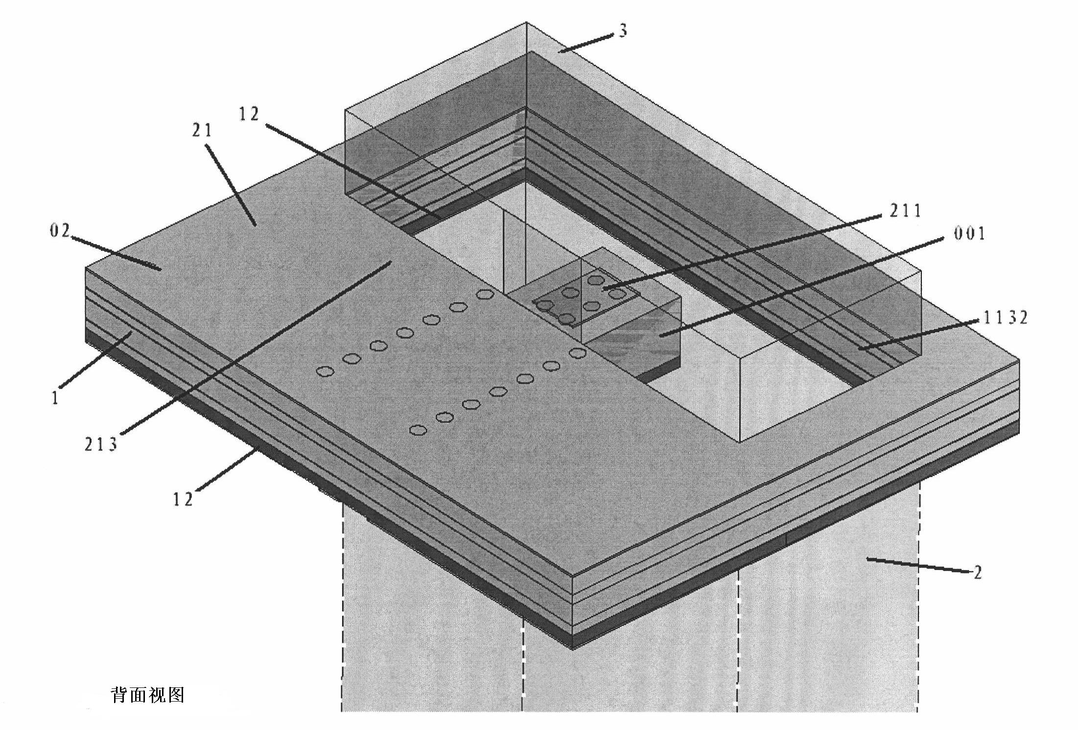
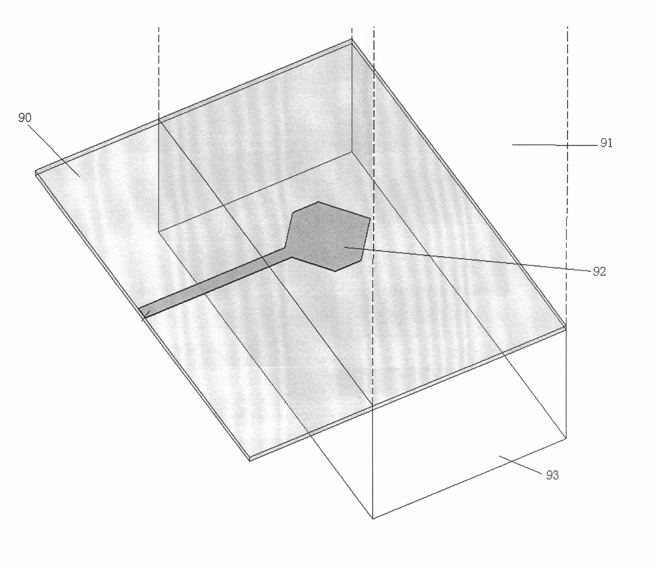
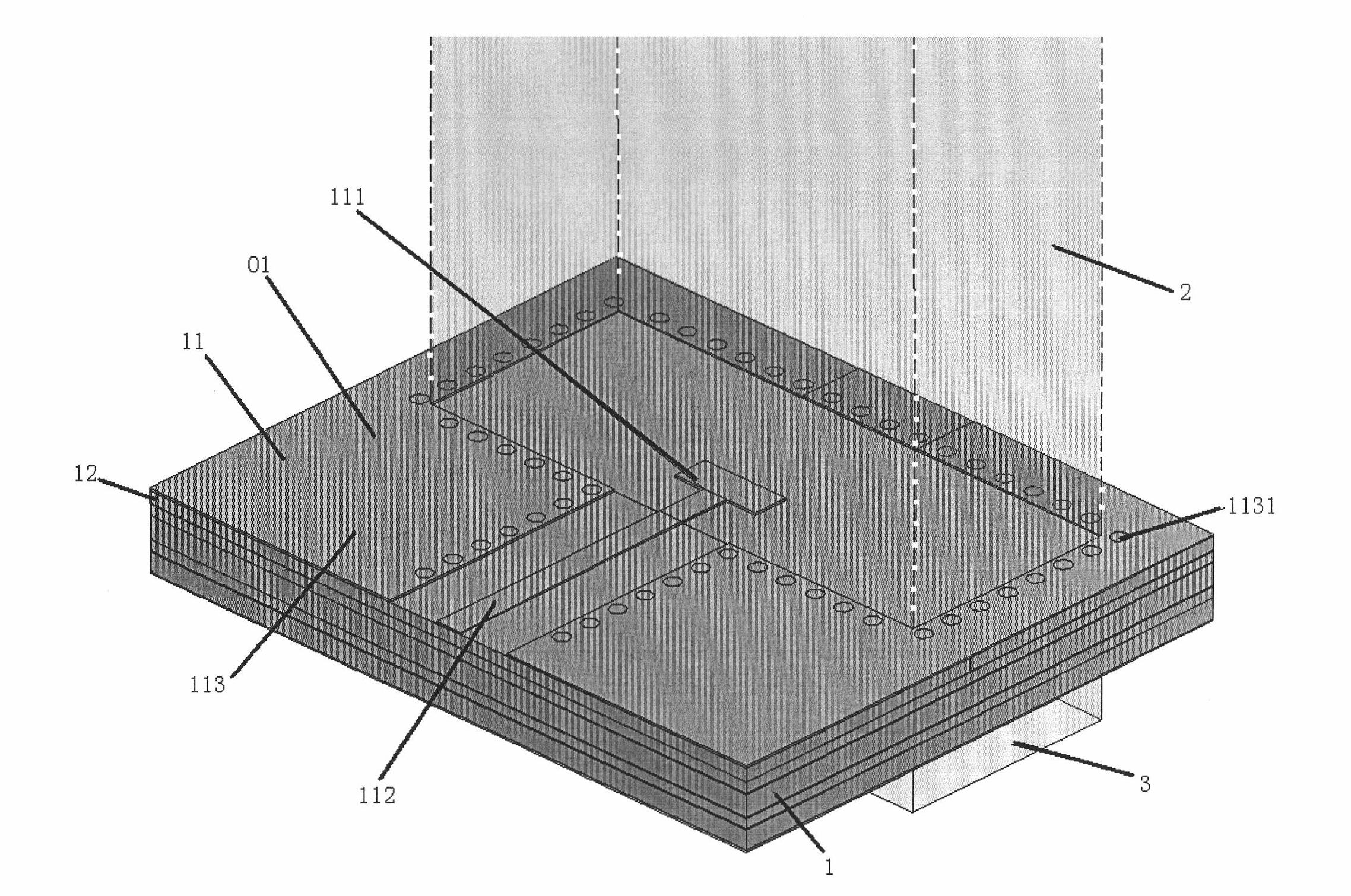
[0022] Such as figure 2 As shown, the embodiment of the present invention provides a waveguide conversion device, including: a multilayer circuit board 1, and waveguide cavities 2 and metal reflection cavities 3 located on both sides of the multilayer circuit board 1, the metal reflection cavity 3 And the waveguide cavity 2 is embedded in the multilayer circuit board 1, the multilayer circuit board 1 is provided with a microstrip line or a stripline, and a matchin...


PUM


Abstract

The embodiment of the invention discloses a waveguide transfer device which comprises a multilayer circuit board, a waveguide cavity and a metallic reflection cavity, wherein the waveguide cavity and the metallic reflection cavity are positioned on two sides of the multilayer circuit board and embedded in the multilayer circuit board, the multilayer circuit board is provided with microstrip lines or strip lines and matching sections connected with the microstrip lines or the strip lines, and the matching sections are positioned in the waveguide cavity.

Description

technical field [0001] The invention relates to the technical field of electronic communication, in particular to a waveguide conversion device. Background technique [0002] Waveguide conversion devices are used in microwave transceiver systems, such as figure 1 As shown, the existing waveguide conversion device is arranged on a two-layer circuit board 90, a microstrip line matching section 92 is arranged on the two-layer circuit board, and a waveguide is arranged on both sides of the two-layer circuit board 90 Cavity 91 and metal reflection cavity 93. [0003] In order to realize the telecommunication connection with the transceiver system on the multi-layer circuit board, the waveguide conversion device needs to be pasted on the multi-layer circuit board or connected to the multi-layer circuit board with a connector. [0004] In the process of realizing the present invention, the inventor finds that the prior art has at least the following disadvantages: [0005] After...

Claims


Application Information

Patent Timeline
Patent Type & Authority Applications(China)
IPC IPC(8): H01P5/107
CPCH01P5/107
Inventor 刘捷郭翠袁文欣余铁柱
Owner HUAWEI TECH CO LTD
Why Eureka
Try Eureka