Structure of resistive random access memory and forming method thereof

A random access memory, resistive technology, applied in electrical components and other directions to achieve the effect of improving uniformity, performance and consistency

Pending Publication Date: 2020-11-17
SEMICON MFG INT (SHANGHAI) CORP +1
View PDF0 Cites 1 Cited by
  • Summary
  • Abstract
  • Description
  • Claims
  • Application Information

AI Technical Summary

Problems solved by technology

[0004] However, the performance of the existing RRAM still needs to be improved

Method used


Image

  • Structure of resistive random access memory and forming method thereof
  • Structure of resistive random access memory and forming method thereof
  • Structure of resistive random access memory and forming method thereof

Examples


Embodiment Construction

[0025] As mentioned in the background, the performance of the RRAM formed in the prior art needs to be improved. The structure of a resistive random access memory is now described and analyzed.

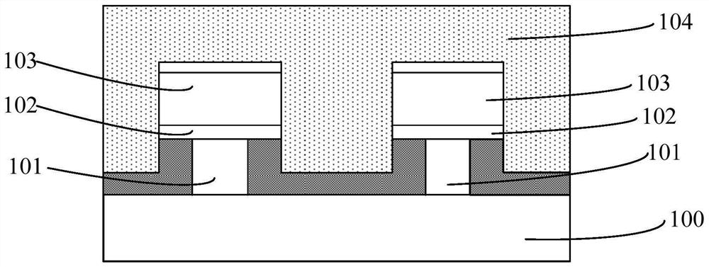
[0026] figure 1 It is a schematic cross-sectional view of a resistive random access memory structure.

[0027] Please refer to figure 1 , provide a substrate 100, the substrate 100 has a resistive random access memory structure, the resistive random access memory structure includes a bottom electrode 101 on the substrate 100, a resistive layer on the bottom electrode 101 102 , a top electrode 103 located on the resistive switch layer 102 , the substrate 100 includes a dielectric layer 104 covering the top and sidewalls of the top electrode 103 and the sidewalls of the resistive switch layer 102 .

[0028] In the resistive random access memory structure, the material of the dielectric layer 104 is silicon oxide, the material of the resistive layer 102 is a transition metal oxide, an...


PUM


Abstract

The invention discloses a structure of a resistive random access memory and a forming method thereof. The forming method comprises the following steps: providing a substrate; forming a bottom electrode on the substrate; forming a resistive layer on the bottom electrode; forming a top electrode on the resistive layer; and forming a first protective layer on the top surface of the top electrode, theside wall surface of the top electrode and the side wall surface of the resistive layer. The performance of the formed resistive random access memory is improved.

Description

technical field [0001] The invention relates to the field of semiconductor manufacturing, in particular to a structure of a resistive random access memory and a forming method thereof. Background technique [0002] Among integrated circuit (IC) devices, resistive random access memory (Resistive Random Access Memory, RRAM for short) is an emerging technology for next-generation non-volatile memory devices. RRAM is a memory structure that includes an array of RRAM cells, each of which stores a small amount of data using resistance instead of charge. Specifically, each resistive random access memory cell includes a resistive material layer, and the resistance of the resistive material layer can be adjusted to display logic "0" or logic "1". [0003] In advanced technology nodes, the size of the components is scaled down and the size of the memory device is reduced accordingly, which requires a corresponding increase in the precision of each process for forming the RRAM to meet...

Claims


Application Information

Patent Timeline
Patent Type & Authority Applications(China)
IPC IPC(8): H01L45/00
CPCH10N70/801H10N70/011
Inventor 杨芸仇圣棻
Owner SEMICON MFG INT (SHANGHAI) CORP
Why Eureka
Try Eureka