Plasma display apparatus using drive circuit

A technology for driving circuits and voltages, applied in the direction of logic circuit coupling/interface, logic circuit connection/interface arrangement, electronic switch, etc. using field effect transistors

Inactive Publication Date: 2011-06-08
RENESAS ELECTRONICS CORP
View PDF5 Cites 2 Cited by
  • Summary
  • Abstract
  • Description
  • Claims
  • Application Information

AI Technical Summary

Problems solved by technology

P-channel MOS transistor MP103 itself generates heat due to a large amount of current (short-circuit current)

Method used


Image

  • Plasma display apparatus using drive circuit
  • Plasma display apparatus using drive circuit
  • Plasma display apparatus using drive circuit

Examples


Embodiment Construction

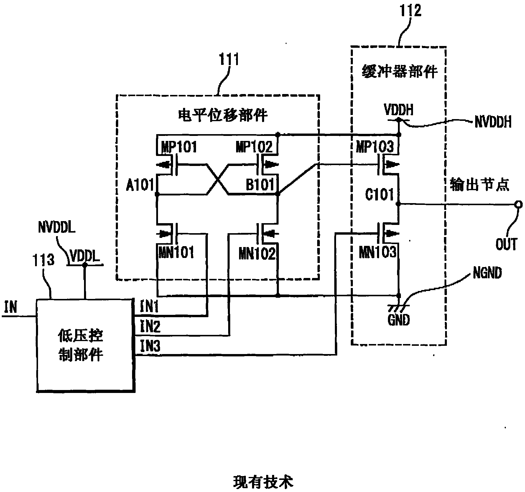
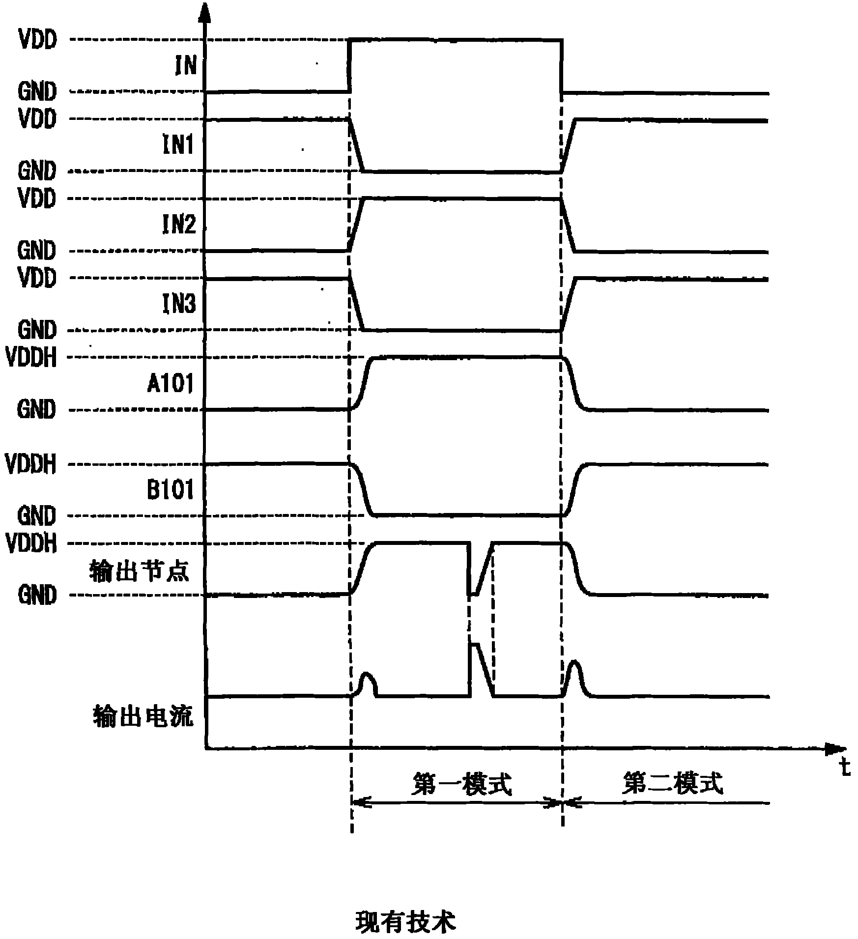
[0031] Hereinafter, a driving circuit according to the present invention will be described with reference to the accompanying drawings. For example, a driving circuit according to an embodiment of the present invention is applied to a data driver of a plasma display device.

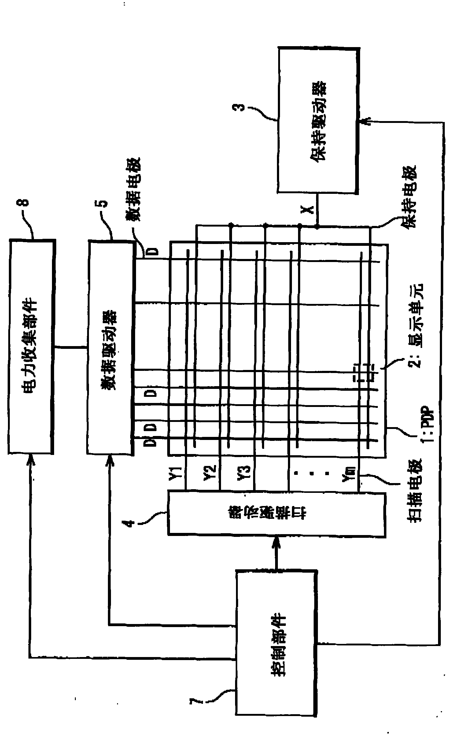
[0032] image 3 The configuration of the plasma display device is shown.

[0033] The plasma display device is provided with a plasma display panel (PDP) 1, a plurality of discharge electrode pairs, and a plurality of data electrodes D. As shown in FIG. One discharge electrode of each of the plurality of discharge electrode pairs is sustain electrode X and the other discharge electrode thereof is a corresponding one of scan electrodes Y1 to Ym (m is an integer equal to or greater than 2). A plurality of data electrodes D are arranged opposite to the plurality of discharge electrode pairs and a display unit 2 as a capacitive element is provided in each of intersections of the plurality of discharge elect...


PUM


Abstract

A plasma display apparatus using a drive circuit. The drive circuit includes: first and second P-channel MOS transistors connected with a first voltage; a first N-channel MOS transistor connected between the first P-channel MOS transistor and a ground voltage, and having a gate connected with a first node and configured to receive a first input signal; and a second N-channel MOS transistor connected between the second P-channel MOS transistor and the ground voltage and having a gate connected with a second node and configured to receive a second input signal. An output P-channel MOS transistor is connected between the first voltage and an output node and has a gate connected with the second node, and an output N-channel MOS transistor is connected between the output node and the second voltage and has a gate supplied with an input signal having a same polarity as that of the first input signal. A P-channel MOS transistor has a source connected with the first node, a drain connected with the output node, and a gate connected with the second node.

Description

technical field [0001] The present invention relates to a drive circuit that performs on / off control of a high breakdown voltage P-channel FET (Field Effect Transistor). Background technique [0002] figure 1 The configuration of a conventional drive circuit shown in Patent Document 1 (Japanese Patent Laid-Open (JP 2006-101490A)) is shown. The first and second power sources NVDDH and NVDDL are connected to the driving circuit to provide a first voltage VDDH and a second voltage VDDL lower than the first voltage VDDH, and a ground voltage GND is also connected to the driving circuit. [0003] A conventional driving circuit is provided with a low voltage control part 113 , a level shift part 111 and a buffer part 112 . [0004] The low voltage control part 113 is connected between the second voltage NVDDL and the ground voltage GND. The low voltage control part 113 uses the third voltage VDDL as a power supply voltage. [0005] The level shift section 111 is provided with ...

Claims


Application Information

Patent Timeline
Patent Type & Authority Applications(China)
IPC IPC(8): G09G3/28G09G3/20G09G3/288G09G3/291G09G3/292G09G3/293G09G3/294G09G3/296G09G3/298H03K17/08H03K19/0185
CPCG09G2330/12G09G2330/04G09G3/296
Inventor 村川真一
Owner RENESAS ELECTRONICS CORP
Why Eureka
Try Eureka