

Stack type differential inductor
A differential inductance, stacking technology, applied in the field of microelectronics, can solve the problem of large area of inductance, achieve the effect of improving quality Q value, reducing production cost, and reducing chip area
- Summary
- Abstract
- Description
- Claims
- Application Information
AI Technical Summary
Problems solved by technology
Method used
Image

Examples
Embodiment Construction
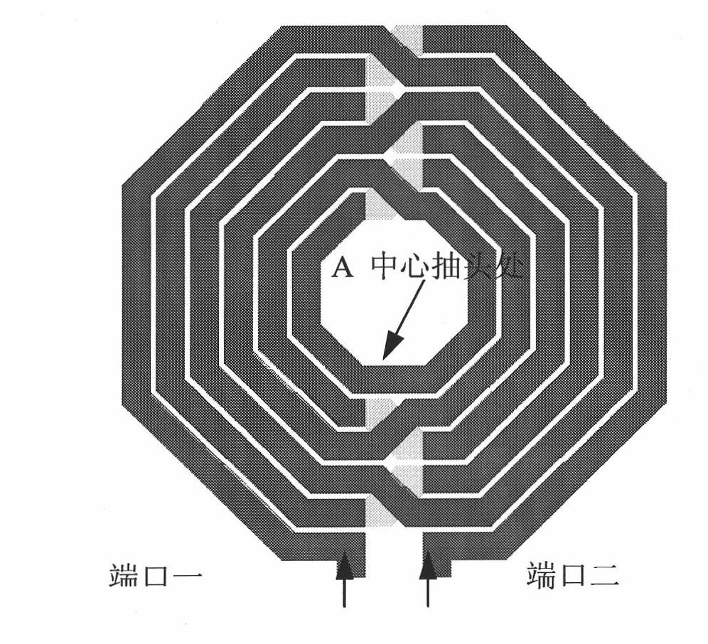
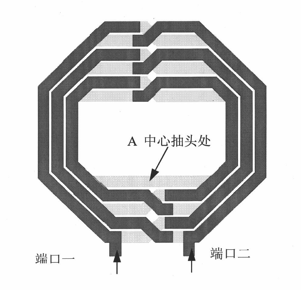
[0014] The stacked differential inductor described in the present invention is a multi-layer structure, including: upper and lower metal coils, the upper and lower metal coils have symmetrical patterns; there are inductor ports on the metal coils; the first layer of metal coils starts from one port of the inductor, passes through A half-circle of metal wiring is connected to another layer of metal wires through an interlayer through hole; another layer of metal is routed through a half circle, connected to the first layer of metal through an interlayer through hole, and the upper and lower layer metal coils are interconnected.
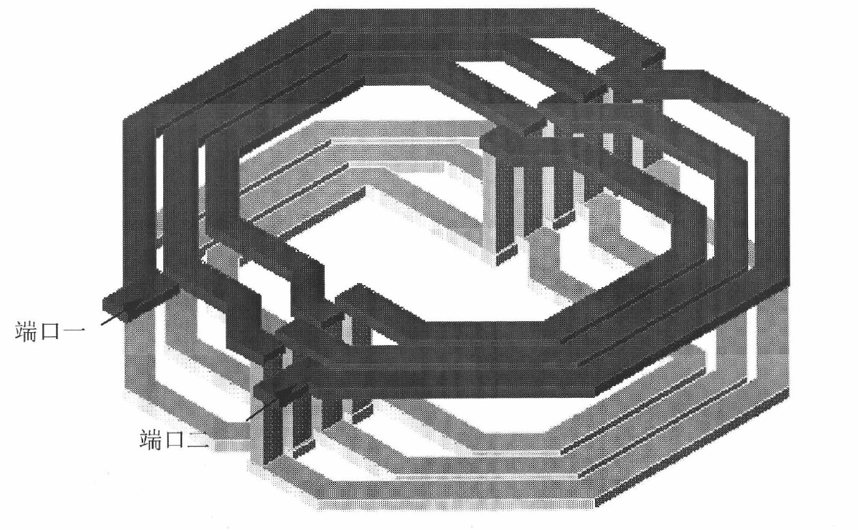
[0015] In more detail, the planar structure of stacked differential inductance with upper and lower layers aligned in the present invention (taking two layers of equal thickness metal and three turns of octagonal inductance as an example), its plan view is shown in figure 2 , its three-dimensional structure see image 3 . from figure 2 It can be se...
PUM
 Abstract
Description
Claims
Application Information