
Housing of electronic device

A technology for electronic devices and shells, which is applied in the direction of electric solid devices, circuits, electrical equipment casings/cabinets/drawers, etc., can solve the problems of low gloss and single structure, achieve elegant appearance, attractiveness, and increase use value and the effect of added value

Inactive Publication Date: 2011-06-15
SHENZHEN FUTAIHONG PRECISION IND CO LTD
View PDF2 Cites 16 Cited by
  • Summary
  • Abstract
  • Description
  • Claims
  • Application Information

AI Technical Summary

Problems solved by technology

However, the above-mentioned metal layer or metal oxide layer formed on the surface of the casing has a single structure and low gloss, making it difficult to make the product present a high gloss and elegant appearance.

Method used


Image

  • Housing of electronic device
  • Housing of electronic device

Examples


Embodiment Construction

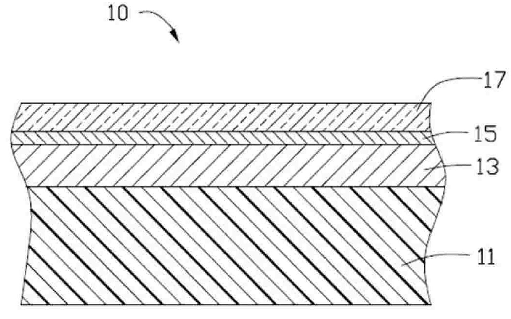
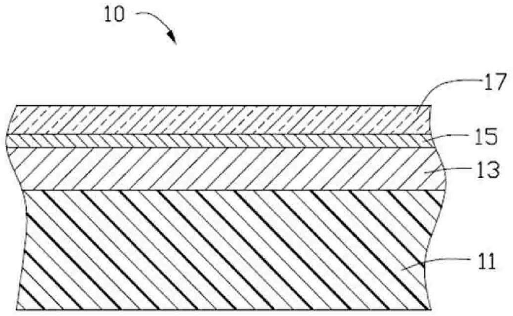
[0007] see figure 1 As shown, the electronic device casing 10 of a preferred embodiment of the present invention includes a substrate 11, a primer layer 13 formed on the substrate 11, a metal oxide film 15 bonded to the primer layer 13, and a metal oxide film 15 bonded to the metal oxide layer. The topcoat layer 17 on the object film 15.

[0008] The base 11 can be an opaque plastic base, which can be made by injection molding. Plastics for injection molding the matrix 11 can be selected from polypropylene (PP), polyamide (PA), polycarbonate (PC), polyethylene terephthalate (PET) and polymethyl methacrylate (PMMA) any of the. The substrate 11 can also be a ceramic substrate. The surface roughness of the substrate 11 is below 60nm. The substrate 11 can be white, black or other colorful colors, preferably white.

[0009] The primer layer 13 can be formed on the surface of the substrate 11 by spraying white, colored or colorless transparent acrylic resin paint. The primer l...


PUM

PropertyMeasurementUnit
surface roughnessaaaaaaaaaa
thicknessaaaaaaaaaa
thicknessaaaaaaaaaa

Abstract

The invention provides a housing of an electronic device. The housing of the electronic device comprises a substrate and a metal oxide film formed on the substrate surface. The roughness value of the substrate surface is below 60 nm. The metal oxide film comprises oxide layers which have different reflective indexes and are arranged alternatively. The oxide layers with different reflective indexes may be a combination of a Ta2O5 oxide layer and a SiO2 oxide layer or a combination of an Nb2O5 oxide layer and a ZrO oxide layer. The surface glossiness value of the housing is 100 to 200 glossiness units.

Description

technical field [0001] The invention relates to an electronic device casing, in particular to an electronic device casing with both metallic texture and high gloss. Background technique [0002] The casings of existing electronic products (such as mobile phones, PDAs, etc.) are often coated with a metal layer or a metal oxide layer to make the product have a metallic texture, thereby attracting consumers' attention. The metal layer is usually formed by non-conductive electroplating, because the metal layer is non-conductive, thereby avoiding interference to signal reception of electronic products. The non-conductive metal layer or metal oxide layer is usually transparent, and after it is formed on the shell, together with the base material of the shell and other paint layers formed on the shell, the shell presents a colorful metallic appearance. Textured look. However, the above-mentioned metal layer or metal oxide layer formed on the surface of the shell has a single stru...

Claims


Application Information

Patent Timeline
Patent Type & Authority Applications(China)
IPC IPC(8): H05K5/00C23C14/34C23C14/08B44C1/00
CPCH01L23/02C23C28/00C23C14/10C23C14/584C23C14/083B44C3/02H01L2924/0002Y10T428/1317Y10T428/13Y10T428/131Y10T428/1352H01L2924/00
Inventor 姜传华杜琪健
Owner SHENZHEN FUTAIHONG PRECISION IND CO LTD
Learn More