Transistor epitaxially growing source/drain region and manufacturing method thereof

An epitaxial growth and manufacturing method technology, applied in semiconductor/solid-state device manufacturing, semiconductor devices, electrical components, etc., can solve the problems affecting the performance of transistor devices, stacking faults of silicon germanium epitaxial layers, etc., to avoid the formation of pit defects , the effect of increasing hole mobility and improving device performance

Inactive Publication Date: 2011-06-22
SEMICON MFG INT (SHANGHAI) CORP
View PDF0 Cites 17 Cited by
  • Summary
  • Abstract
  • Description
  • Claims
  • Application Information

AI Technical Summary

Problems solved by technology

[0005] The technical problem to be solved by the present invention is to provide a transistor and a manufacturing method for epitaxially growing source / drain regions, so as to solve the problem of pit defects and pit defects in the silicon germanium epitaxial layer during the process of growing the silicon germanium epitaxial layer to form the device source / drain region. Stacking fault, a problem that affects the performance of transistor devices

Method used


Image

  • Transistor epitaxially growing source/drain region and manufacturing method thereof
  • Transistor epitaxially growing source/drain region and manufacturing method thereof
  • Transistor epitaxially growing source/drain region and manufacturing method thereof

Examples


Embodiment Construction

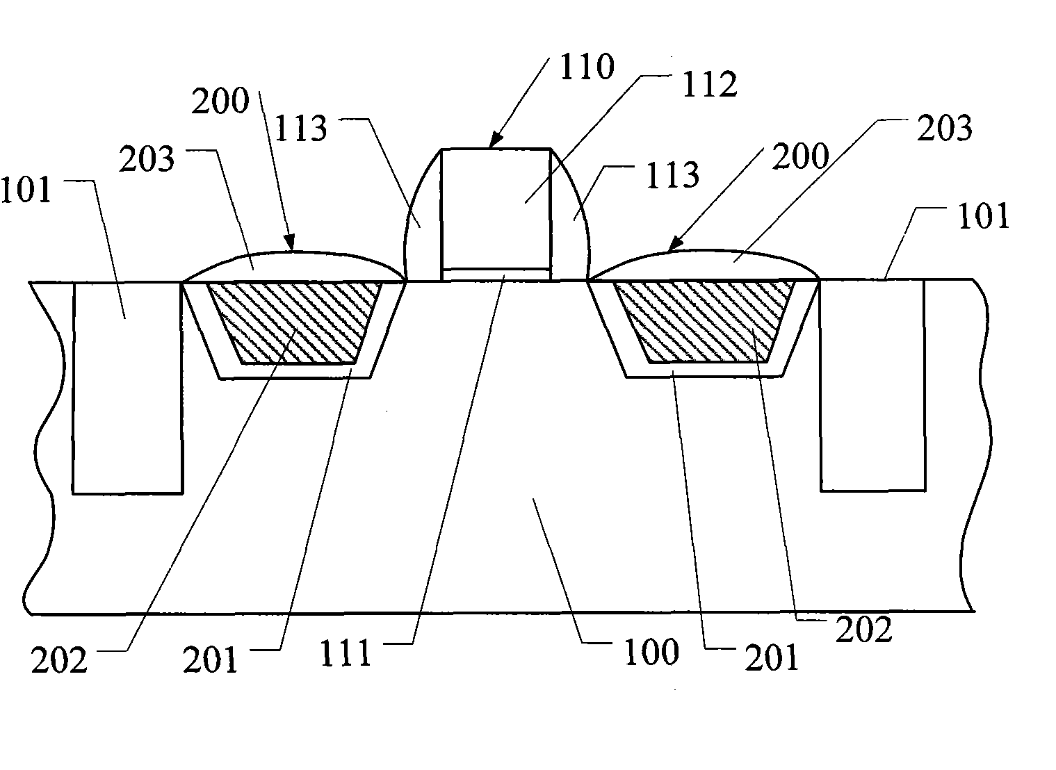
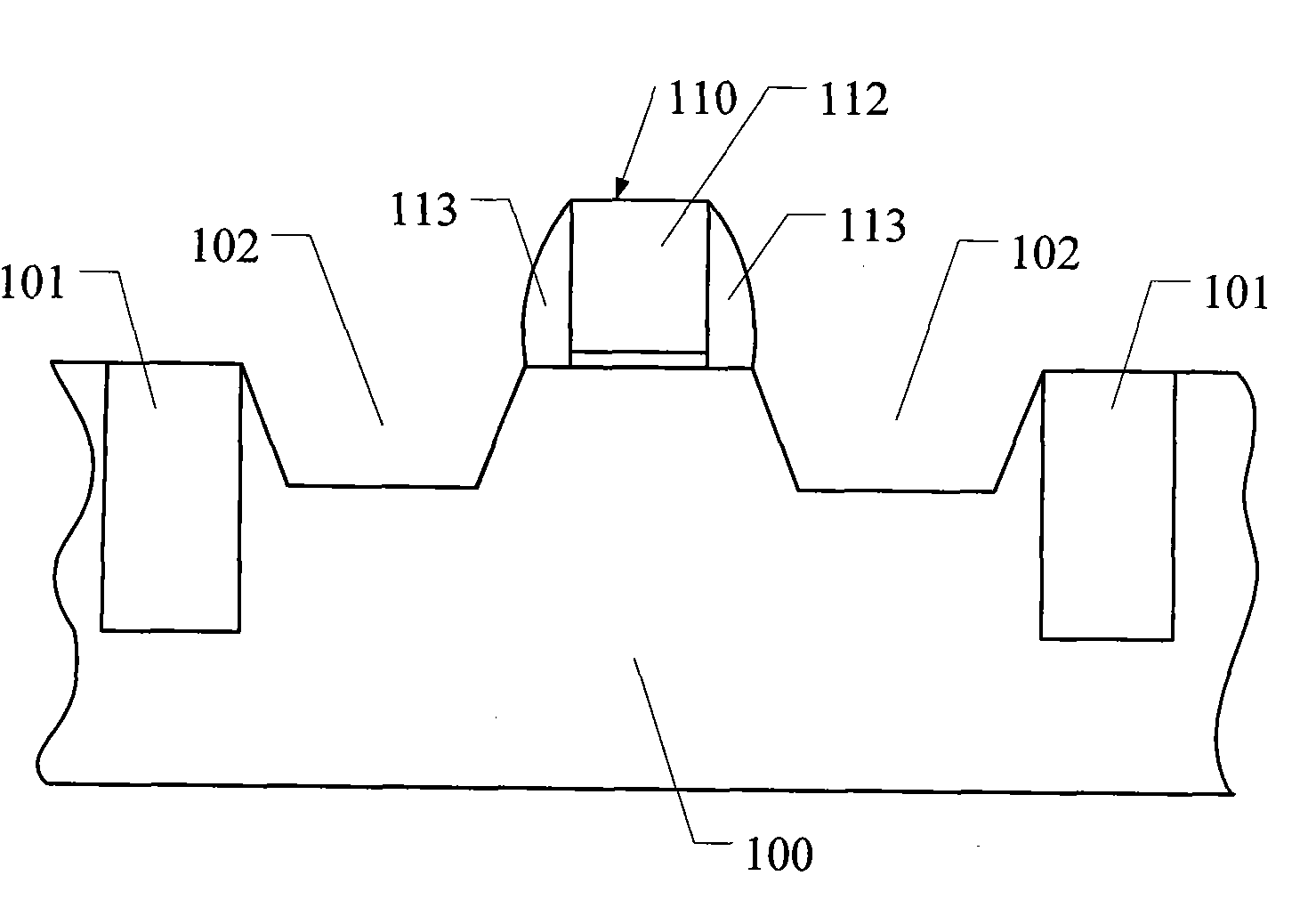
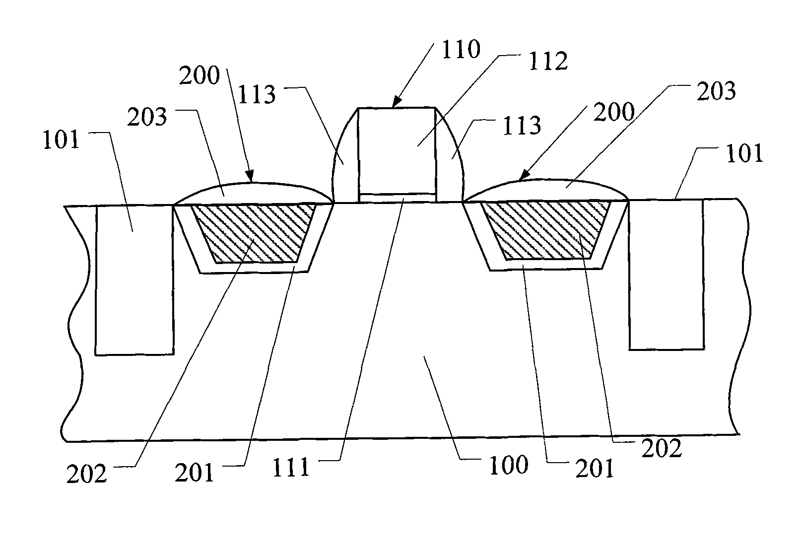
[0036] In order to make the above objects, features and advantages of the present invention more comprehensible, specific implementations of the present invention will be described in detail below in conjunction with the accompanying drawings.

[0037] A kind of epitaxially grown source / drain region transistor and its manufacturing method described in the present invention can be realized in various alternative ways, and the following is an illustration through a preferred embodiment, of course, the present invention is not limited to this specific embodiment, Common substitutions known to those skilled in the art undoubtedly fall within the protection scope of the present invention.

[0038] Secondly, the present invention is described in detail using schematic diagrams. When describing the embodiments of the present invention in detail, for the sake of illustration, the schematic diagrams are not partially enlarged according to the general scale, which should not be used as a...


PUM


Abstract

The invention provides a transistor epitaxially growing a source / drain region, comprising a substrate, a grid structure, a source region and a drain region, wherein the grid structure is positioned on the substrate; the source region and the drain region are formed in the substrate and positioned at both sides of the grid structure; the source region and the drain region comprise doped first homoepitaxial layers, doped heteroepitaxial layers and doped second homoepitaxial layers, wherein the doped heteroepitaxial layers are positioned on the doped first homoepitaxial layers, and the doped second homoepitaxial layers are positioned on the doped heteroepitaxial layers. The invention also provides a method for manufacturing the transistor. The transistor epitaxially growing the source / drain region can effectively reduce the defects of stacking faults and recesses.

Description

technical field [0001] The invention relates to the field of semiconductor integrated circuit manufacturing, in particular to a MOS transistor with epitaxially grown source / drain regions. Background technique [0002] When the semiconductor integrated circuit enters the deep sub-micron process, the size of the components is gradually reduced, so that the operation speed of the entire integrated circuit will be effectively improved. However, when the size of the device is further reduced, in the case of metal oxide semiconductor transistors, the resistance and parasitic capacitance of the gate and source / drain will increase accordingly, which will reduce the size of the device. Improvement of overall circuit performance is hindered. If the device size continues to shrink, the area of ​​the entire device will be occupied by the ohmic contact of the source / drain, which sets the upper limit of the integrated circuit integration. [0003] At present, the industry has applied th...

Claims


Application Information

Patent Timeline
Patent Type & Authority Applications(China)
IPC IPC(8): H01L29/78H01L29/08H01L21/336H01L21/28
Inventor 何有丰胡亚兰
Owner SEMICON MFG INT (SHANGHAI) CORP
Why Eureka
Try Eureka