MEMS devices

A device and component technology, applied in the field of packaging device formation, can solve the problems of time-consuming, expensive non-customized parts, etc.

Inactive Publication Date: 2011-06-22
NXP BV
View PDF4 Cites 5 Cited by
  • Summary
  • Abstract
  • Description
  • Claims
  • Application Information

AI Technical Summary

Problems solved by technology

[0011] Selection of non-custom parts is an expensive and time-consuming process

Method used


Image

  • MEMS devices
  • MEMS devices
  • MEMS devices

Examples


Embodiment Construction

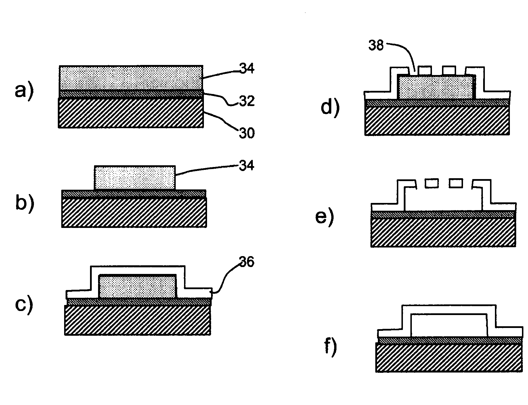
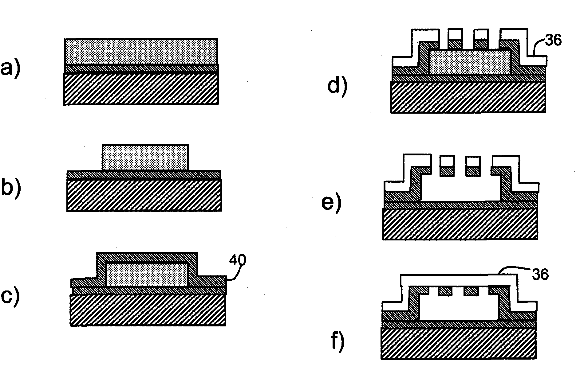
[0038] The present invention proposes a method of manufacturing a MEMS device, wherein a closed cavity is formed on said MEMS device element. A sacrificial layer is used, which is removed through the holes in the cover layer. The pores are then closed by an annealing process.

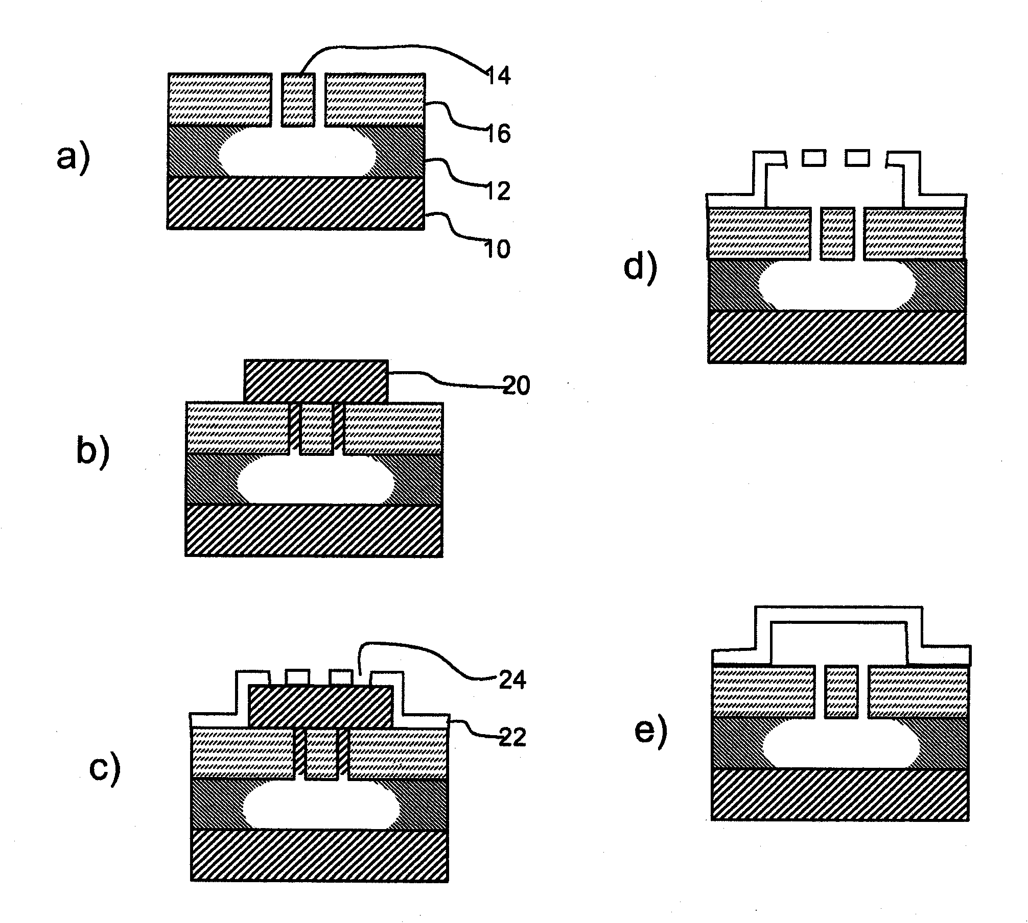
[0039] figure 1 The method of the invention is schematically shown.

[0040] figure 1 a shows a complete surface micromechanical device, in this example in the form of a resonator. The device comprises a silicon substrate 10 ; a silicon oxide layer 12 forming a cavity beneath the resonator mass; and the resonator mass 14 formed in a silicon layer 16 .

[0041] The present invention does not require changes to the fabrication of the MEMS device, and any conventional technique may be used. For example, the MEMS device may be a resonator, capacitor or switch. Typically the device has movable parts which need to be carefully protected by packaging, in this example the device has a suspended resonator ...


PUM

PropertyMeasurementUnit
thicknessaaaaaaaaaa
thicknessaaaaaaaaaa

Abstract

A method of manufacturing a MEMS device comprises forming a MEMS device element (14). A sacrificial layer (20) is provided over the device element and a package cover layer (22) is provided over the sacrificial layer. The sacrificial layer is removed using at least one opening (22) in the cover layer and the at least one opening (24) is sealed by an anneal process.

Description

technical field [0001] The invention relates to a MEMS device, in particular to the formation of a packaged device. Background technique [0002] MEMS technology is gradually being used in integrated circuits. However, as a result of the difficulty in providing suitable and cost-effective packaging, various product concepts have not been realized in practice. [0003] There are many contributing factors to the high cost of MEMS device and system packaging. The three basic factors are: [0004] - For MEMS systems with complex geometries, specific tooling and fixtures are required for proper packaging and efficient assembly of parts and assemblies with dimensions below a few millimeters. [0005] - High density MEMS devices and systems make the requirements for reliable packaging vary significantly from product to product. For example, vacuum packaging for hermeticity is necessary in many cases. [0006] -The small size of parts and assemblies in MEMS devices and systems ...

Claims


Application Information

Patent Timeline
Patent Type & Authority Applications(China)
IPC IPC(8): B81C1/00
CPCB81C2203/0145B81C1/00293
Inventor 格雷亚·J·A·M·费尔海登菲利普·默尼耶-贝拉德约翰内斯·J·T·M·唐克斯
Owner NXP BV
Why Eureka
Try Eureka