An optical element for a light emitting device and a method of manufacturing thereof

A technology of optical components and light-emitting devices, applied in chemical instruments and methods, luminescent materials, electrical components, etc., can solve problems such as changes, deviations, and functional degradation of optical components, and achieve high durability, high preparation performance, and improved grinding ability Effect

Active Publication Date: 2011-06-22
SIGNIFY HLDG BV
View PDF1 Cites 17 Cited by
  • Summary
  • Abstract
  • Description
  • Claims
  • Application Information

AI Technical Summary

Problems solved by technology

This can lead to undesired deviations from the normal light intensity distribution
[0009] In addition, chemical interactions between the wavelength conversion layer and the scattering layer may lead to functional degradation of the optical element, such as destroyed luminescence or changes in emission color

Method used


Image

  • An optical element for a light emitting device and a method of manufacturing thereof
  • An optical element for a light emitting device and a method of manufacturing thereof

Examples


example 1

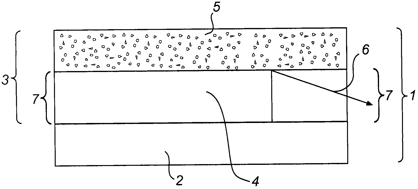
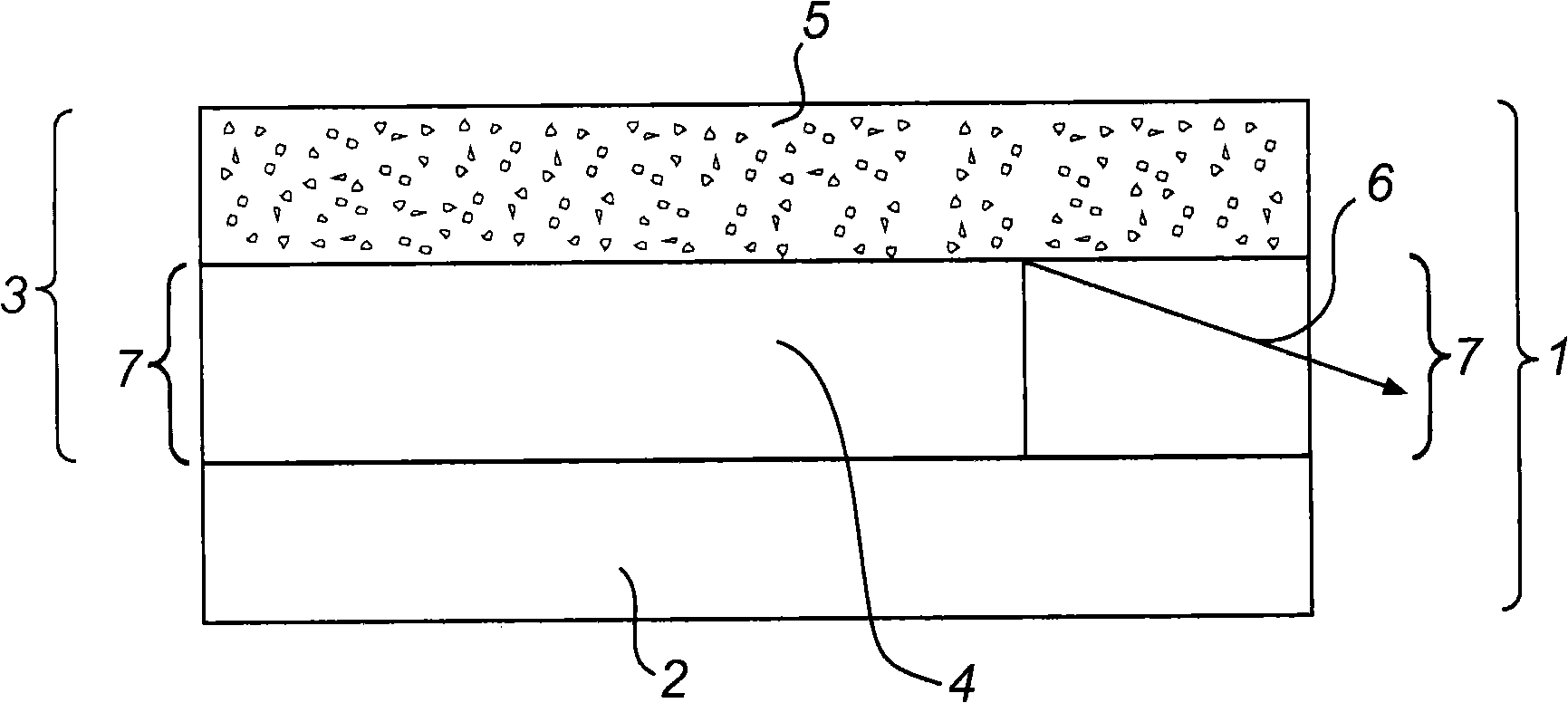
[0054] The preparation of an optical element according to the invention comprises a first layer (wavelength conversion layer), and a second layer with scattering properties, wherein the optical element is based on Y 3 Al 5 o 12 .

[0055] The following oxide compositions were used for the green body:

[0056] Y 2 o 3 , specific surface area 15m 2 / g, available from Rodia;

[0057] Al 2 o 3 , specific surface area 8m 2 / g, available from Reynolds / Malakoff;

[0058] CeO 2 , specific surface area 4m 2 / g, available from Rodia; and

[0059] Gd 2 o 3 (in the case of a red-shifted wavelength conversion layer), the specific surface area is 17m 2 / g.

[0060] Alternatively, will be used for sintering based on Y 3 Al 5 o 12 An appropriate flux for ceramic materials SiO 2 Added to the first layer at a concentration of 200-2000 ppm and added to the second layer at a concentration of 0-500 ppm. The first layer is doped with 0.01-2% Ce.

[0061] The green body is pres...


PUM

PropertyMeasurementUnit
reflectivityaaaaaaaaaa
diameteraaaaaaaaaa
porosityaaaaaaaaaa

Abstract

The present invention relates to an optical element for a light emitting device, wherein the optical element comprises a sintered ceramic body (3) comprising a wavelength converting layer (4) and a scattering layer (5), and to a method of manufacturing thereof. More specifically, the invention relates to an optical element, comprising a sintered ceramic body (3) of a first layer (4) and a second layer (5) arranged on the first layer, wherein the first layer comprises a wavelength converting material, the porosity of the second layer is higher than the porosity of the first layer, and pores inthe second layer are arranged to provide scattering of a light beam. The method for manufacturing of the optical element comprises providing a green body comprising a first layer of a first material and a second layer of a second material; and co-sintering said layers into a sintered ceramic body; the compositions of the first and second layer are adapted such that after sintering, the porosity of the second layer is higher than the porosity of the first layer, and pores in said second layer are arranged to provide scattering of a light beam.

Description

technical field [0001] The present invention relates to an optical element for a light emitting device and a manufacturing method thereof, wherein the optical element includes a sintered ceramic body including a wavelength conversion layer and a scattering layer. Background technique [0002] The light emitting device comprises at least one light emitting diode (LED), which is usually arranged together with an optical element. The optical element typically includes a wavelength converting layer including phosphors and / or layers that redirect emitted light. The primary light emitted by the LED can thus be influenced in various ways. [0003] Top-emitting LEDs refer to light-emitting diodes that have an optical element in which the light generated by the LED is emitted at the upper surface of the optical element. Properties such as high transparency and optimal wavelength conversion are desired for optical elements in top-emitting LEDs. This is preferably done by using an o...

Claims


Application Information

Patent Timeline
Patent Type & Authority Applications(China)
IPC IPC(8): H01L33/00
CPCC04B2235/604C04B2235/3418H01L33/44H01L33/507C04B2235/3229C04B2237/586C04B2235/77C04B2237/704B32B18/00C04B2235/3225C04B2235/6562C09K11/7774C04B2235/3224C04B35/44C04B2237/343C04B2235/5409C04B2235/6565H01L33/505H01L2933/0091Y10T156/10Y10T428/249969H01L33/50
Inventor J·F·M·希勒森H·A·M·范哈尔H·J·B·雅格特O·J·斯泰吉尔曼
Owner SIGNIFY HLDG BV
Why Eureka
Try Eureka