

Method and system for detecting defect of material based on electron pair effect
A technology for electron pair effect and detection of materials, which is applied in the direction of material analysis using radiation
- Summary
- Abstract
- Description
- Claims
- Application Information
AI Technical Summary
Problems solved by technology
Method used
Image

Examples
Embodiment Construction
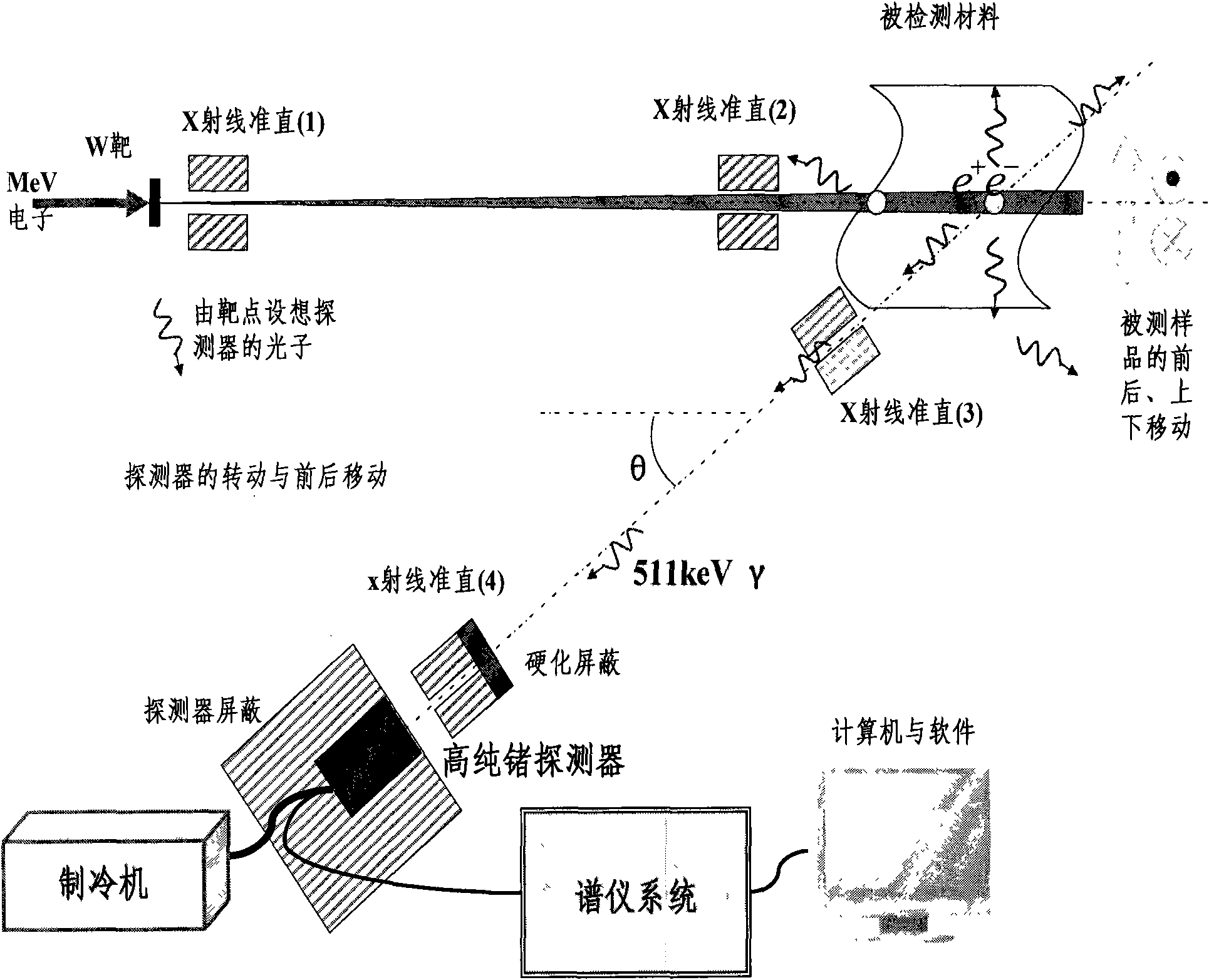
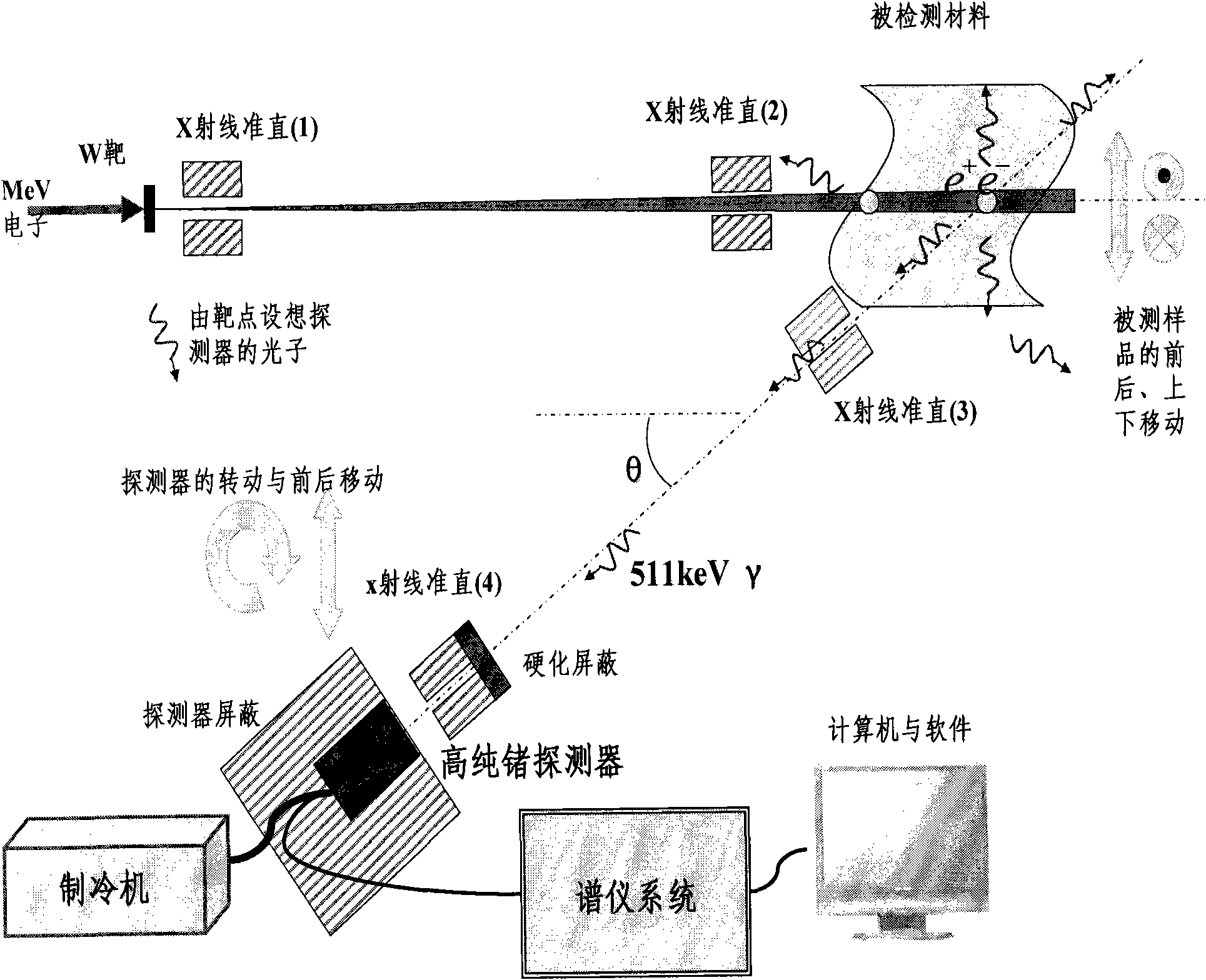
[0010] figure 1 A schematic diagram of a preferred embodiment of the method and system of the present invention is shown. As shown in the figure, after the electrons of several MeV produced by the electron accelerator bombard the tungsten target, bremsstrahlung X-rays with an energy value lower than 7 MeV will be produced, and these X-rays will pass through the X-ray collimator (1) and shoot to The detected material is collimated for the second time through the X-ray collimator (2), and then irradiated to a certain local position of the detected material.
[0011] X-rays injected into the material to be tested can undergo various reactions with it, including photoelectric effect, Compton scattering, electron pair effect, Rayleigh scattering, etc. Positrons and negative electrons are generated when X-rays interact with the material to be detected. The generated positrons are decelerated and slowed down in the detected object. When there are certain defects in the material, th...
PUM
 Abstract
Description
Claims
Application Information