Transistor and manufacturing method thereof

A manufacturing method and transistor technology, applied in semiconductor/solid-state device manufacturing, semiconductor devices, electrical components, etc., can solve problems such as carrier mobility decline

Active Publication Date: 2011-07-06
INST OF MICROELECTRONICS CHINESE ACAD OF SCI
View PDF1 Cites 9 Cited by
  • Summary
  • Abstract
  • Description
  • Claims
  • Application Information

AI Technical Summary

Problems solved by technology

This shows that the interface layer wil

Method used


Image

  • Transistor and manufacturing method thereof
  • Transistor and manufacturing method thereof
  • Transistor and manufacturing method thereof

Examples


Embodiment Construction

[0040] Various features and advantages of the present invention will be described in detail below with reference to the detailed description and drawings thereof. Also, please note that the various features in the drawings are not drawn to scale. Descriptions of well-known components and processing techniques are omitted so as not to obscure the present invention. The specific embodiments described here are only used to better understand the present invention and help those skilled in the art to implement the present invention. Therefore, the detailed description should not limit the scope of the invention.

[0041] As mentioned above, the present invention relates to a transistor, more specifically a transistor with an asymmetric gate replacement, the relevant characteristics of which will be described in detail here. Note that similar or corresponding parts will be denoted by the same reference numerals.

[0042] according to Figure 4, an exemplary transistor structure ...


PUM

PropertyMeasurementUnit
Thicknessaaaaaaaaaa
Thicknessaaaaaaaaaa

Abstract

The invention discloses a transistor. The transistor comprises a base with a channel region, a source region, a drain region, a gate high-K dielectric layer and an interface layer, wherein the source region and the drain region are positioned at the two ends of the channel region of the base; the gate high-K dielectric layer is formed on a top layer of the base above the channel region between the source region and the drain region; the interface layer is positioned below the gate high-K dielectric layer; a first part of the interface layer is close to a source, and a second part of the interface layer is close to a drain; and an equivalent oxide layer of the first part is thicker than an equivalent oxide layer of a second layer. An asymmetric interface layer is formed by an asymmetrically substituted metal gate and is thinner on the side of the drain and is thicker on the side of the source. A short channel effect is more important on the thinner drain side, and the asymmetric interface layer contributes to controlling the short channel effect; and on the thicker source side, carrier mobility has larger influence on a device, and the asymmetric interface layer can prevent a carrier mobility rate from being reduced. In addition, the asymmetrically substituted metal gate can also form an asymmetric metal work function.

Description

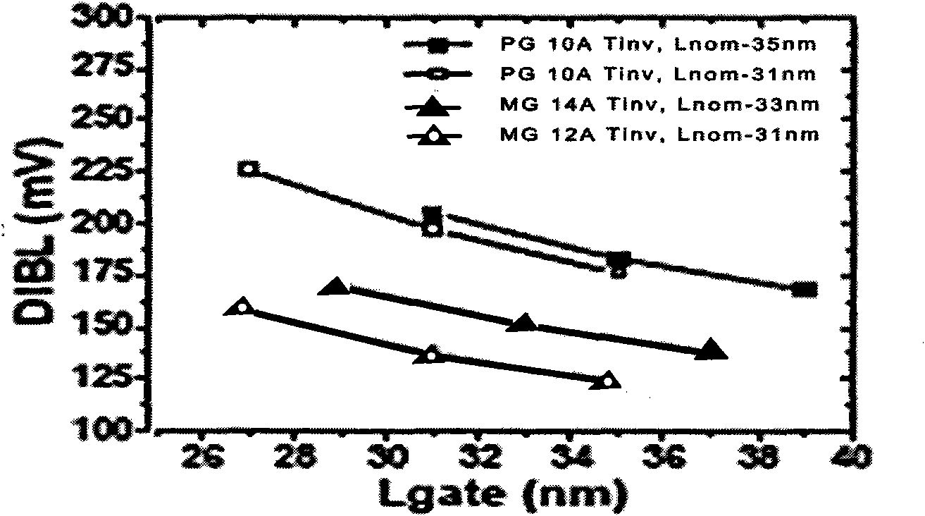
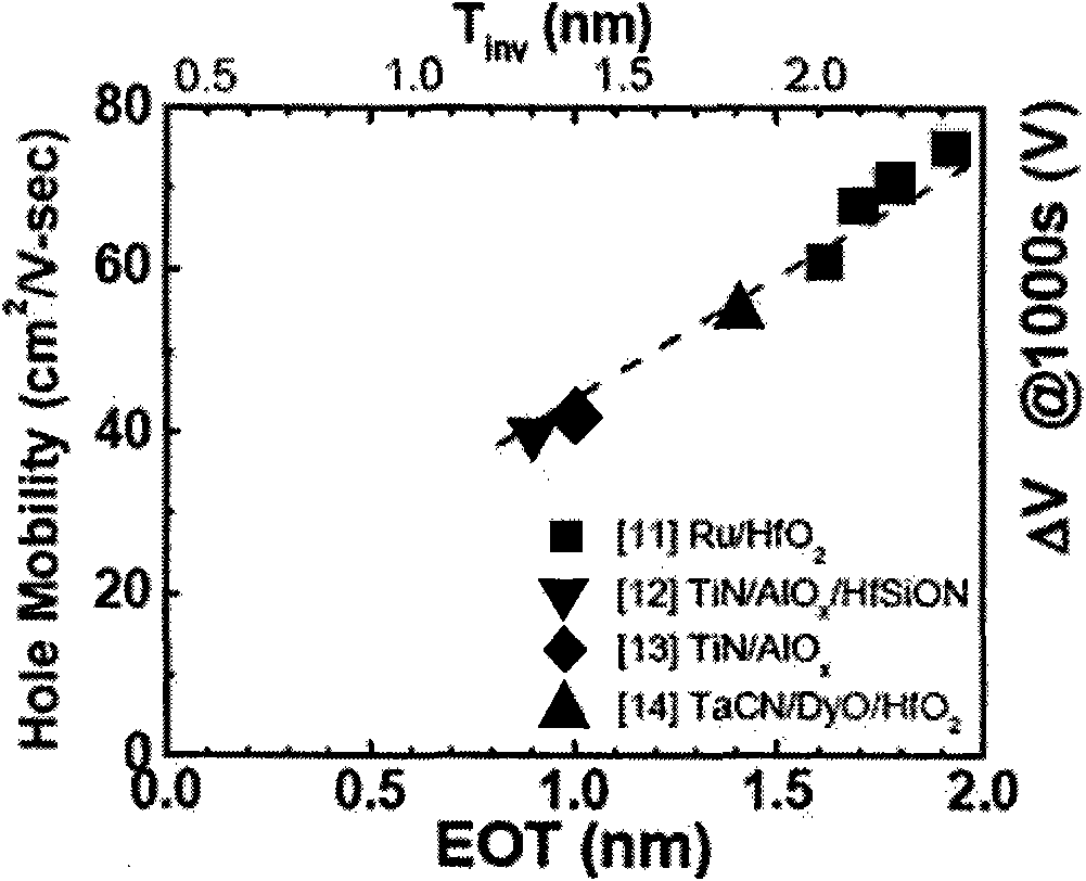
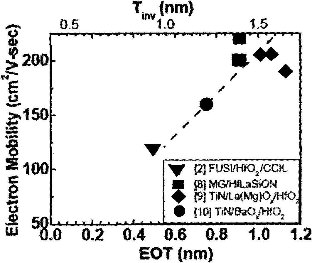
technical field [0001] The present invention mainly relates to a transistor, especially a transistor with an asymmetric gate structure and a manufacturing method thereof. Background technique [0002] The main problem limiting the further scaling of metal-oxide-semiconductor (MOS) transistors is the short-channel effect (SCE), and this phenomenon mainly occurs when the channel length is less than 0.1 micron. Device failures include, but are not limited to, DIBL (lower drain-induced carrier barrier, ie, low source-drain breakdown voltage), subthreshold leakage, and threshold instability. These problems are collectively referred to as the short channel effect, which is mainly related to the equivalent oxide thickness (EOT) of the interface layer, and a thin EOT is beneficial to control the short channel effect (especially at the drain end), as cited in the citation High-Performance High- K / Metal Gates for 45nm CMOS and Beyond with Gate-First Processing (M. Chudziket al. VLSI ...

Claims


Application Information

Patent Timeline
IPC IPC(8): H01L29/78H01L21/336
CPCH01L29/513H01L29/4983H01L21/28105H01L29/512H01L29/66545H01L29/517H01L21/283H01L29/78
Inventor 尹海洲骆志炯朱慧珑
Owner INST OF MICROELECTRONICS CHINESE ACAD OF SCI
Why Eureka
Try Eureka