
Attenuation phase shift mask

A technology of attenuation phase shift and mask, applied in the field of lithography, can solve the problem that the attenuation phase shift mask cannot meet the design requirements, and achieve the effect of large process window

Active Publication Date: 2012-12-05
SEMICON MFG INT (SHANGHAI) CORP +1
View PDF1 Cites 0 Cited by
  • Summary
  • Abstract
  • Description
  • Claims
  • Application Information

AI Technical Summary

Problems solved by technology

Attenuated phase-shift masks with a single transmittance cannot meet current design requirements, especially for designs with both memory devices and logic devices

Method used


Image

  • Attenuation phase shift mask
  • Attenuation phase shift mask
  • Attenuation phase shift mask

Examples


Embodiment Construction

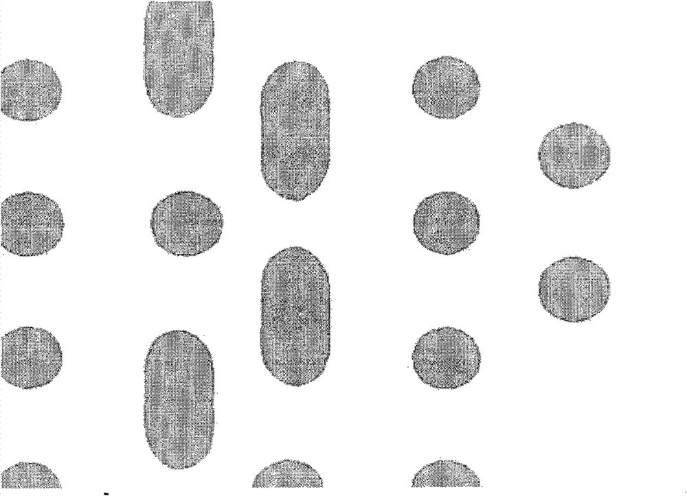
[0018] In semiconductor processes, such as logic devices, which include both static random access (SRAM) components and random logic (Random Logic) components, when using photolithographic technology to make contact holes, the design is realized by attenuating the phase shift mask Graphic transfer.

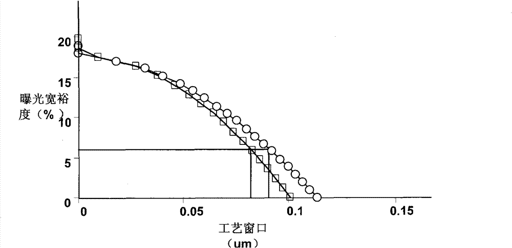
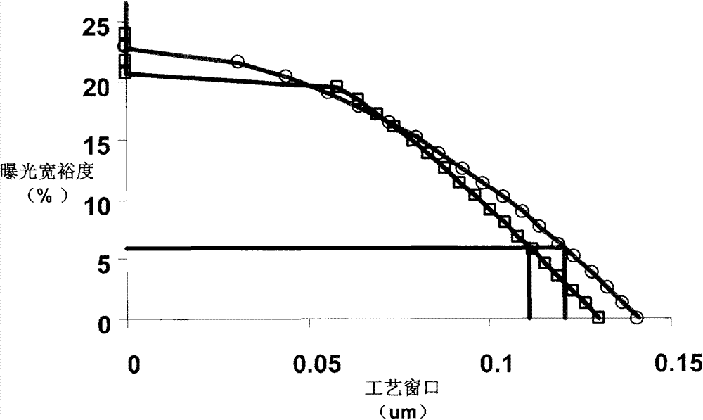
[0019] In the prior art, if an attenuated phase-shift mask with a single light transmittance is used, it will lead to a contradiction between the process window and the side lobe effect. For example, with an exposure margin of 6%, refer to figure 1 with figure 2 , when using an attenuated phase-shift mask with a light transmittance of 6%, see the curve formed by the small squares, the process window of the static random memory component is 0.082um, the process window of the random logic component is 0.11um, and when using For an attenuated phase-shift mask with a light transmittance of 12%, see the curve formed by the small circles, the process window of the static random memor...


PUM

PropertyMeasurementUnit
transmittivityaaaaaaaaaa

Abstract

The invention discloses an attenuation phase shift mask, which has set transmittance and comprises a first phase shift layer and a second phase shift layer, wherein the first phase shift layer has first transmittance; the second phase shift layer is positioned on the surface of the first phase shift layer, the second phase shift layer is made of a material with second transmittance, and the second transmittance is determined according to the set transmittance and the first transmittance; and the first phase shift layer or the combination of the first phase shift layer and the second phase shift layer form a phase shift layer, and rays transmitting the phase shift layer and rays transmitting the gaps for forming an image are subjected to 180-degree phase shift by adjusting the thicknesses or the thickness sum of the first phase shift layer and the second phase shift layer. The attenuation phase shift mask can adjust the transmittance, has a wider application range, and reduces the number of side lobe patterns at the same time of meeting the requirement of a process window.

Description

technical field [0001] This invention relates to photolithography, and in particular to attenuated phase shift masks. Background technique [0002] With the rapid development of integrated circuit design, the size of design graphics is shrinking day by day, and the optical proximity effect is becoming more and more obvious. More and more optical technologies and optical proximity correction technologies are applied to the photolithography process. For example, corresponding to the miniaturization of patterns, the exposure light sources used for photolithography are increasingly shortened. However, shortening the exposure wavelength will reduce the depth of focus while improving the sharpness, thereby reducing the stability of the process. In order to ensure the accuracy of photolithographic patterns, Phase Shift Mask (PSM, Phase ShiftMask) technology is increasingly used. [0003] Theoretically, the electric field E1 at the light-transmitting slit in the reticle should be ...

Claims


Application Information

Patent Timeline
Patent Type & Authority Patents(China)
IPC IPC(8): G03F1/32
Inventor 朴世镇
Owner SEMICON MFG INT (SHANGHAI) CORP
Learn More