Chip radiation method, and related device and system

A technology of chip heat dissipation and heat sink, which is applied in the manufacture of electrical components, circuits, printed circuits, etc., can solve the problems of difficult installation and fixing, bulky heat sink, and large area of ​​heat dissipation holes, and achieve low cost, small size, and easy The effect of installation

Inactive Publication Date: 2011-07-20
HUAWEI DEVICE CO LTD
View PDF3 Cites 20 Cited by
  • Summary
  • Abstract
  • Description
  • Claims
  • Application Information

AI Technical Summary

Problems solved by technology

[0004] Although the above method has better heat dissipation performance, due to the large area of ​​the heat dissipation hole, it is generally suitable for the heat dissipation of chips with a large bottom area and no pins on the bottom. For chips with a small bottom area or a chip with pins on the bottom ( Such as BGA-packaged chips) cannot be applied. At the same time, the heat sink with bosses is relatively heavy, and it is relatively difficult to install and fix.

Method used


Image

  • Chip radiation method, and related device and system
  • Chip radiation method, and related device and system
  • Chip radiation method, and related device and system

Examples


Embodiment Construction

[0024] Embodiments of the present invention provide a chip heat dissipation method, a related device and a system, which are used to improve the heat dissipation efficiency of a chip on the premise of low cost and easy installation.

[0025] In order to make the purpose, features and advantages of the present invention more obvious and understandable, the technical solutions in the embodiments of the present invention will be clearly and completely described below in conjunction with the accompanying drawings in the embodiments of the present invention. Obviously, the described The embodiments are only some of the embodiments of the present invention, but not all of them. Based on the embodiments of the present invention, all other embodiments obtained by persons of ordinary skill in the art without making creative efforts belong to the protection scope of the present invention.

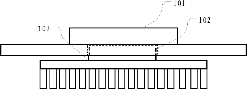
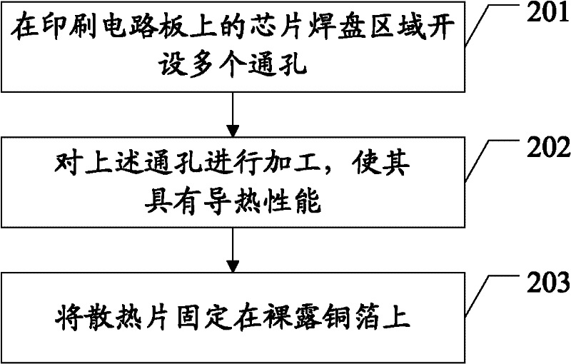
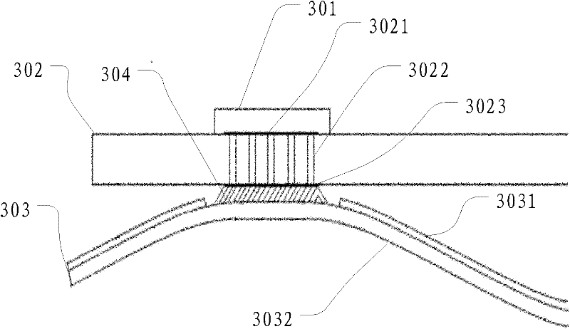
[0026] The chip cooling method in the embodiment of the present invention is described below, ple...


PUM


Abstract

The embodiment of the invention discloses a chip radiation method, and a related device and system. The chip radiation method comprises steps as follows: a chip pad region on a printed circuit board is provided with a plurality of through holes, and the other surface of the chip pad region on the printed circuit board is provided with a bare metal foil; the through holes are processed so as to have heat-conducting property; and radiating fins are fixed on the bare metal foil. The technical scheme disclosed by the invention can effectively implement radiation of various chips; and the volume of the radiating fins can be easily set to be small enough so that the radiating fins have the characteristic of low cost, and are easy to install.

Description

technical field [0001] The invention relates to the technical field of electronic communication, in particular to a chip heat dissipation method, a related device and a system. Background technique [0002] Chips usually generate a lot of heat during their work, and when the chip is not cooled, most of the heat generated will be transferred to the printed circuit board (PCB, Printed Circuit Board) where it is located. For example, research has found that, When a chip using a small square planar package (QFP, Quad Flat Package) is not treated for heat dissipation, more than 60% of the heat loss generated during operation will be transferred to the PCB where it is located through the bottom of the chip. However, due to the small size of most chip packages, the contact surface between the bottom heat dissipation pad and the circuit board is extremely small, so the heat transfer capability to the circuit board is extremely limited, and for some QFP packages, square flat no-lead ...

Claims


Application Information

Patent Timeline
Patent Type & Authority Applications(China)
IPC IPC(8): H01L21/48H05K1/02H05K3/00H01L23/367
Inventor 阳军
Owner HUAWEI DEVICE CO LTD
Why Eureka
Try Eureka