

Film deposition apparatus
A film-forming device and film-forming technology, which are used in gaseous chemical plating, coatings, electrical components, etc., can solve problems such as the inability to suppress the mixing of the first and second reaction gases, the inability to solve problems, and the inability to achieve sufficient treatment. Long time, high film forming speed and good film quality
- Summary
- Abstract
- Description
- Claims
- Application Information
AI Technical Summary
Problems solved by technology
Method used
Image

Examples
Embodiment Construction
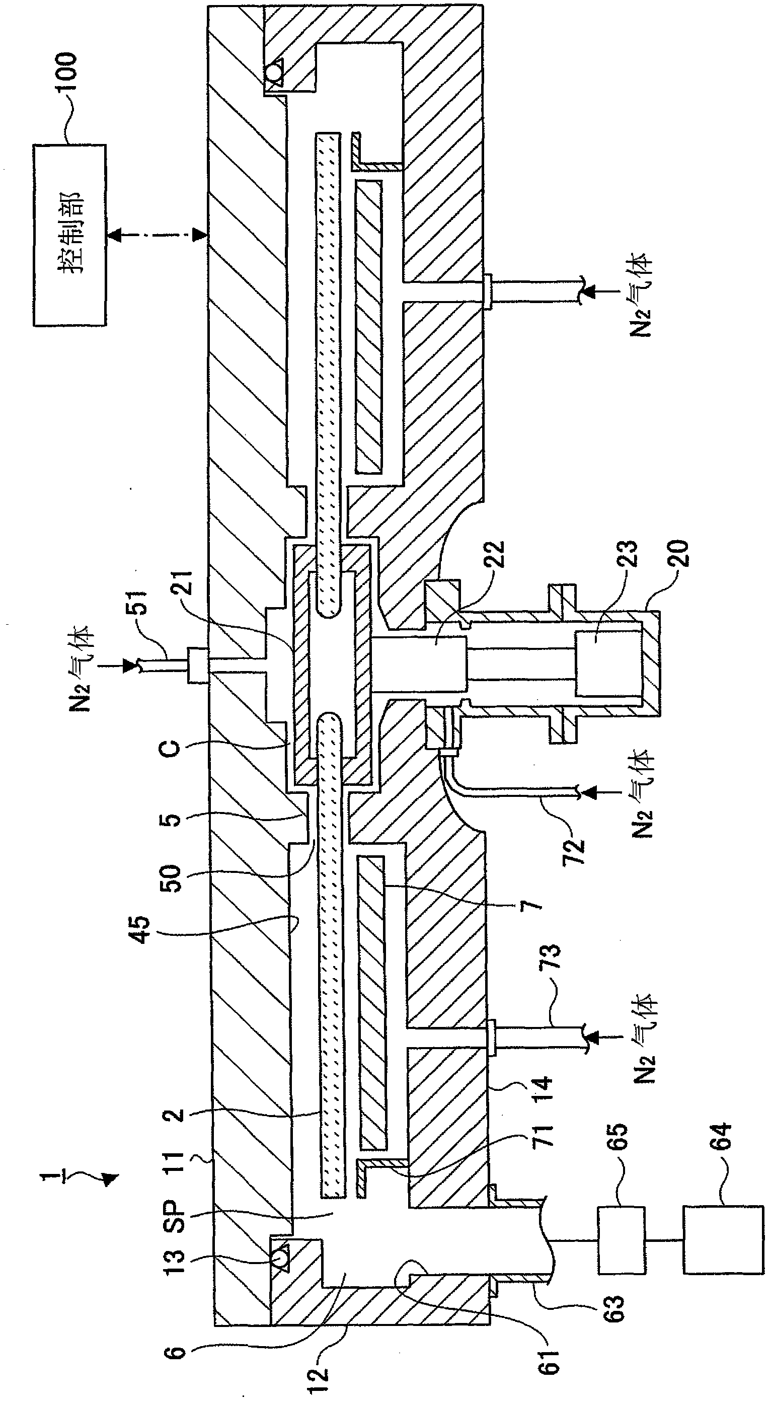
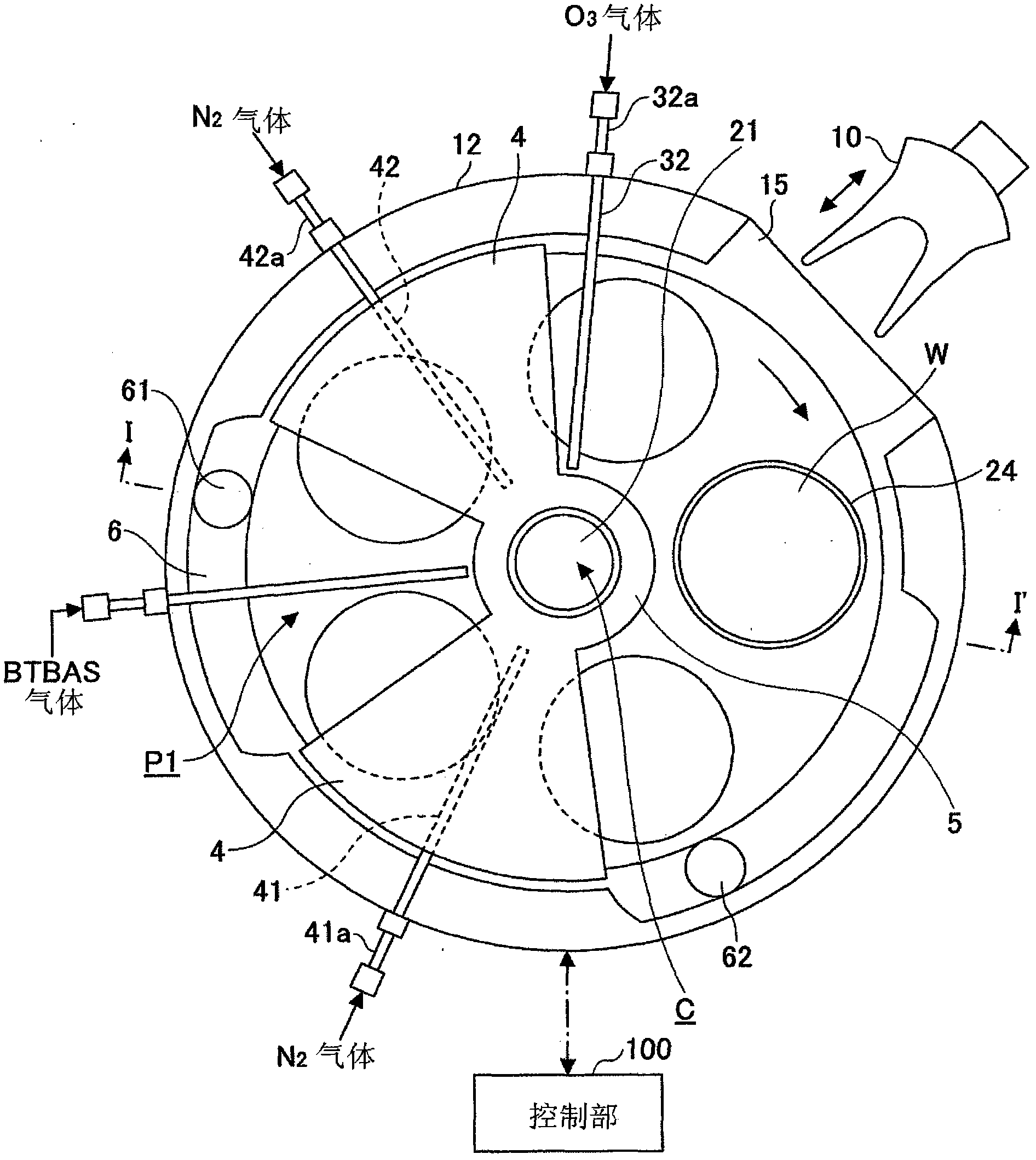
[0039] Such as figure 1 ( image 3 As shown in the cross-sectional view of I-I′ in ), the film forming apparatus according to the embodiment of the present invention includes a flat vacuum container 1 having a substantially circular planar shape (planar view). The film forming apparatus further includes a rotary table 2 disposed in the vacuum container 1 and having a rotation center at the center of the vacuum container 1 . The top plate 11 of the vacuum container 1 can be separated from the container main body 12 . The top plate 11 is pressed against the side of the container main body 12 through a sealing member, such as an O-ring 13, to maintain an airtight state by utilizing the internal decompression state. The driving mechanism lifts the top plate 11 upwards.
[0040] The center portion of the turntable 2 is fixed to a cylindrical core 21 fixed to an upper end of a rotating shaft 22 extending in the vertical direction. The rotating shaft 22 penetrates the bottom sur...
PUM
| Property | Measurement | Unit |
|---|---|---|
| length | aaaaa | aaaaa |
| length | aaaaa | aaaaa |
| length | aaaaa | aaaaa |
Abstract
Description
Claims
Application Information