High-speed and high-resolution number collecting device of banknote sorting machine and identification method

A high-resolution, acquisition device technology, applied in the field of image processing, can solve the problems of banknote running speed limitation, high light source performance requirements, and large volume, and achieve low cost, low light source performance requirements, and small size.

Inactive Publication Date: 2011-08-03
HARBIN INST OF TECH
View PDF4 Cites 33 Cited by
  • Summary
  • Abstract
  • Description
  • Claims
  • Application Information

AI Technical Summary

Problems solved by technology

When the part of the number area is in two adjacent areas, the number area needs to be spliced, which is difficult to deal with, resulting in unsatisfactory recognition accuracy
In addition, the use of CCD image sensors requires high light source performance and large object distances, resulting in large equipment and unattractive appearance.
The other is to use a contact image sensor (CIS) to collect banknote images, and use a digital signal processor (DSP) to identify banknote numbers, such as the solutions provided by ZL200610155872.0 and 20100104848.0 patents. This type of method is due to the integration time of contact image sensors. The constraint of the minimum value limits the running speed of banknotes
In addition, the imaging quality of the contact image sensor is poor, and the existing banknote number positioning and segmentation methods cannot obtain accurate positioning and segmentation positions when banknotes are depreciated and polluted, resulting in the inability to obtain ideal banknote number recognition results

Method used


Image

  • High-speed and high-resolution number collecting device of banknote sorting machine and identification method
  • High-speed and high-resolution number collecting device of banknote sorting machine and identification method
  • High-speed and high-resolution number collecting device of banknote sorting machine and identification method

Examples


Embodiment 1

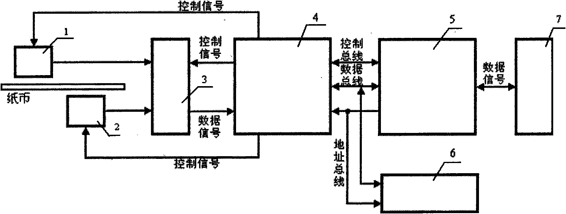
[0015] Example 1: Combining figure 1 , the present invention is a banknote sorting machine high-speed high-resolution number acquisition device, which is composed of a first contact image sensor (1), a second contact image sensor (2), a multi-channel analog-to-digital converter chip (3), Composed of a programmable logic chip (4), a digital signal processor chip (5), a dynamic memory chip (6) and a communication structure chip (7), the first contact image sensor (1), the second contact image sensor ( 2) respectively connected to the multi-channel analog-to-digital converter chip (3), the multi-channel analog-to-digital converter chip (3) is connected to the programmable logic chip (4), and the programmable logic chip (4) is respectively connected to the digital signal processor chip ( 5) and the dynamic memory chip (6), the digital signal processor chip (5) is connected with the communication structure chip (7).

[0016] The recognition method realized by the high-speed and hi...

Embodiment 2

[0017] Example 2: Combining figure 1 The high-speed and high-resolution number collection device of the banknote sorting machine includes first and second contact image sensors, a multi-channel analog-to-digital conversion chip, a programmable logic chip, a dynamic memory chip, a digital signal processor chip and a communication interface chip. The first and second contact image sensors are respectively connected to a multi-channel analog-to-digital conversion chip and a programmable logic chip, and the programmable logic chip is respectively connected to a multi-channel analog-to-digital conversion chip, a digital signal processor chip, and a dynamic memory chip, and the digital signal The processor chip is connected with the communication interface chip; the multi-channel analog-to-digital conversion chip is an AD9822 chip, the programmable logic chip is a Xilinx FPGA XC3S200 chip, the digital signal processor chip TITMS320C6000 series chip, and the dynamic memory chip is an ...

Embodiment 3

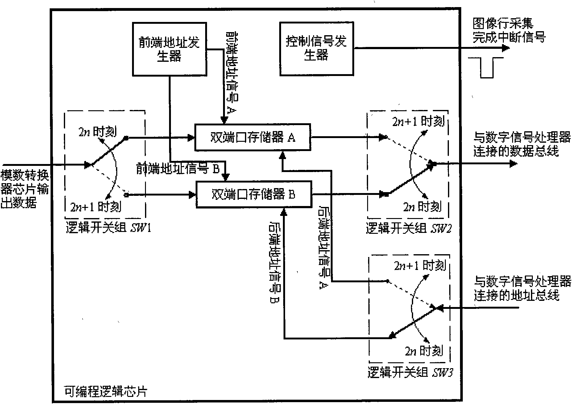
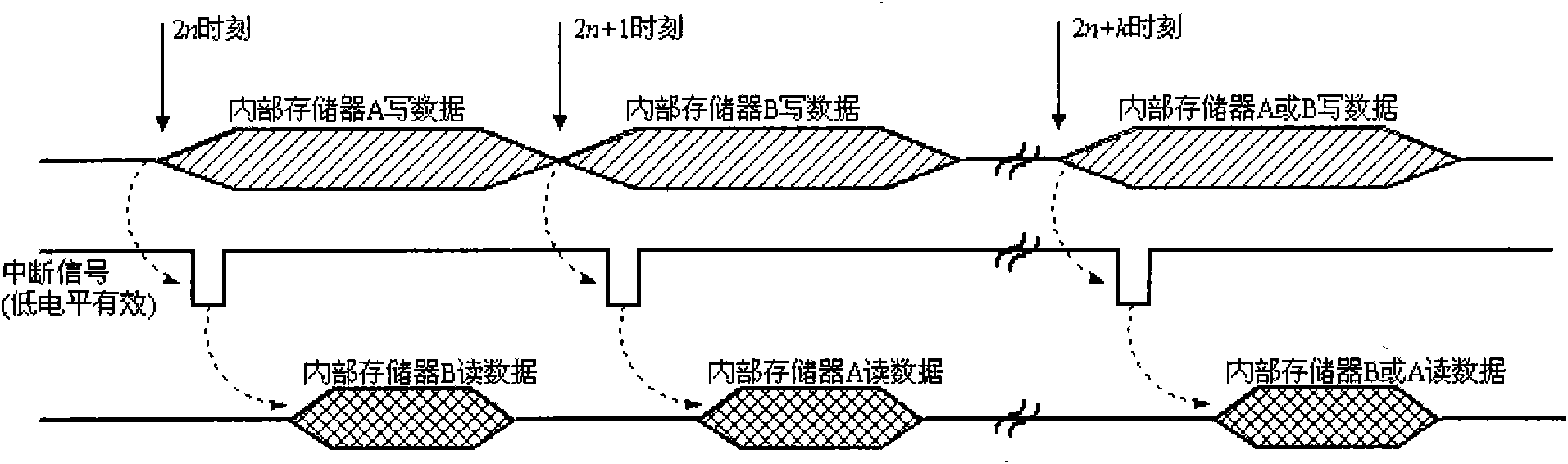
[0019] Example 3: Binding figure 1 -- Figure 6 , The high-speed and high-resolution number acquisition device of the banknote sorting machine includes first and second contact image sensors (CIS), multi-channel analog-to-digital converter chips, programmable logic chips, digital signal processor chips, dynamic memory chips and communication structures chip. Two contact image sensors placed staggeredly can collect the images of the upper and lower sides of the banknote at the same time, at least one side image includes the banknote number area; the analog-to-digital converter chip converts the output voltage signals of the two contact image sensors into digits The signal is used as the input signal of the programmable logic chip; the programmable logic chip completes the parallel execution of image acquisition and data transmission between the programmable logic chip and the digital signal processor chip under the high-speed operation of banknotes, and obtains High-resolutio...


PUM


Abstract

The invention provides a high-speed and high-resolution number collecting device of a banknote sorting machine and an identification method. The high-speed and high-resolution number collecting device of the banknote sorting machine comprises image sensors, a multichannel A/D (analog to digital) converter chip, a programmable logic chip, a digital signal processor chip, a dynamic memory chip and a communication structure chip, wherein the image sensors are respectively connected with the multichannel A/D converter chip, the multichannel A/D converter chip is connected with the programmable logic chip, and the programmable logic chip is respectively connected with the digital signal processor chip and the dynamic memory chip. The invention realizes the high-resolution collection to banknote images under the condition of high-speed operation of the banknotes. The contact type image sensors have the advantages of low cost, small volume and low requirements for light source performance. Positioning and cutting thresholds are not needed to be set in the identification method of banknote numbers, so that an accurate positioning and cutting position and ideal identification results can be obtained when the banknotes are depreciated and polluted.

Description

(1) Technical field [0001] The invention relates to image processing technology, in particular to a high-speed and high-resolution number collection device for a banknote sorting machine and a recognition method thereof. (2) Background technology [0002] The existing banknote sorting machine number collection devices are divided into two categories, one is to use the CCD area array image sensor to collect the image of the banknote number area, the device requires a high number of CCD lenses, such as the 201001044234. The device collects images of four areas in two directions of the banknote respectively. These four areas cannot cover all the images of the banknote. The algorithm searches these four areas to determine the location of the number. When the part of the number area is in two adjacent areas, the number area needs to be spliced, which is very difficult to handle, resulting in unsatisfactory recognition accuracy. In addition, the use of CCD image sensors has high ...

Claims


Application Information

Patent Timeline
Patent Type & Authority Applications(China)
IPC IPC(8): G07D13/00
Inventor 唐降龙刘鹏金野程丹松刘家锋吴锐刘松波黄剑华佟喜峰黄庆成赵巍
Owner HARBIN INST OF TECH
Why Eureka
Try Eureka